Specific Process Knowledge/Lithography/Resist
Feedback to this page: click here
This section is under construction 
UV Resist
UV resist comparison table
Comparison of specifications and feature space of the standard UV photoresists available at DTU Nanolab.
| Resist | AZ 5214E | AZ MiR 701 | AZ nLOF 2020 | AZ 4562 | SU-8 | TI Spray |
|---|---|---|---|---|---|---|
| Resist tone |
|
Positive | Negative | Positive | Negative |
|
| Thickness range | 1.5 - 4.2 µm | 1.5 - 4 µm | 1.5 - 4 µm | 5 - 10 µm | 1 - 200 µm | 0.5 - 5 µm |
| Coating tool |
Automatic spin coaters:
Manual spin coaters:
Spray coater |
Automatic spin coaters:
Manual spin coaters:
Spray coater |
Automatic spin coaters:
Manual spin coaters:
Spray coater |
Automatic spin coaters:
Manual spin coaters:
|
Manual spin coaters:
|
Spray coater |
| Spectral sensitivity | 310 - 420 nm | 310 - 445 nm | 310 - 380 nm | 310 - 445 nm | 300 - 375 nm | 310 - 440 nm |
| Exposure tool |
|
|
|
|
|
|
| Developer |
|
|
|
AZ 726 MIF (2.38% TMAH) |
mr-DEV 600 (PGMEA) |
AZ 726 MIF (2.38% TMAH) |
| Development rinse agent | DIW | DIW | DIW | DIW | IPA | DIW |
| Remover |
|
|
|
Remover 1165 (NMP) |
|
|
| Comments | Good adhesion for wet etch | High selectivity for dry etch | Negative sidewalls for lift-off | For processes with resist thickness between 6 µm and 25 µm |
|
TI spray resist is an image reversal resist, similar to AZ 5214E. The process flow will be similar to the process flows for 5214, except for the coating step. The exposure dose and development will depend on the specific process. |
Process flow examples
Comparison of specifications and feature space of the standard UV photoresists available at DTU Nanolab. These are just examples and may contain obsolete information regarding exposure dose, etc.
| Resist | AZ 5214E | AZ MIR 701 | AZ nLOF 2020 | AZ 4562 | SU-8 | Ti Spray |
|---|---|---|---|---|---|---|
| Maskless aligner |
NB! Most of the process knowledge about SU-8 is based in research groups |
|||||
| Mask aligner |
NB! Most of the process knowledge about SU-8 is based in research groups |
Other process flows: Chip on carrier: A procedure for UV lithography on a chip using automatic coater and developer.
Exposure dose

During exposure of the resist, the photoinitiator, or photo-active component, reacts with the exposure light, and starts the reaction which makes the resist develop in the developer.
In a positive resist, it makes the resist become soluble in the developer. In a negative resist, usually assisted by thermal energy in the post-exposure bake (PEB), it makes the resist insoluble in the developer. The amount of light required to fully develop the resist in the development process, is the exposure dose.
The optimal exposure dose is a function of many parameters, including the type of resist, the resist thickness, and the sensitivity of the resist.
Resist sensitivity
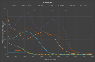
The resist sensitivity is a measure of how efficiently it reacts to the exposure light. Spectral sensitivity is the sensitivity of the resist as a function of wavelength. It is usually given simply as the range from the wavelength below which absorption in the resist material makes lithography impractical to the wavelength at which the photoinitiator is no longer efficiently activated.
Within the sensitivity range, the optical absorption is commonly used as a measure of sensitivity. A high absorption coefficient signifies a high sensitivity, as the light is absorbed by the photoinitiator. Because of spectral sensitivity, the optimal dose of a given resist type and thickness is also a function of the spectral distribution of the exposure light, i.e. the equipment used for the exposure. Using a combination of experience, calculation and assumptions, it may be possible to estimate the dose for an exposure equipment, if the exposure dose is already known on another equipment.
Due to reflection and refraction at the interface between the resist and the substrate, the optimal dose may also be a function of the type of substrate used. Unless otherwise stated, the exposure doses given below are for standard silicon wafers.
Apart from the already mentioned factors, the optimal dose also depends on the developer chemistry and the parameters used in the development process. Finally, the requirements to the lithographic process in terms of resolution, bias (line broadening), etch selectivity, side wall angle, etc. may narrow down, or widen, the process window. The exposure doses given in the sections below should be used as a starting point for individual fabrication process development.
Due to the process of bleaching, where the absorption of the resist changes during exposure, the exposure dose is unfortunately not always constant at different intensities of the exposure light. The exposure time is thus not always a linear function of the exposure intensity.
Calculate exposure time
In the maskless aligners, the dose is set directly as a process parameter in the job. In mask aligners, on the other hand, the parameter that is set is the exposure time, i.e. how long the shutter is open during the exposure.
The exposure dose, D [J/m2], in terms if exposure light intensity I [W/m2] and exposure time t [s], is given by:
Since the intensity is specific to the spectral sensitivity of the sensor used to measure the exposure light, and the exposure time is specific to the spectral distribution of the exposure light (cf. spectral sensitivity), this dose is specific to the combination of exposure source and optical sensor.
Given an exposure dose, the exposure time, t, is calculated as:
It is important to keep in mind that this exposure time is valid only for a specific combination of exposure source and optical sensor, as well as for a specific development process.
Exposure dose for mask aligners
Information about the exposure dose for mask aligners can be found here.
Exposure dose for maskless aligners
Information about the exposure dose for maskless aligners can be found here.
Exposure dose when using AZ 351B developer (NaOH)
Information about the exposure dose when using AZ 351B developer can be found here.
DUV Resist
The content on this page, including all images and pictures, was created by DTU Nanolab staff, unless otherwise stated.
Feedback to this page: click here
Spin coater: Süss stepper

This spinner is dedicated for spinning DUV resists. The spinner is fully automatic and can run up to 25 substrates in a batch 4", 6", and 8" size (8" requires tool change). The machine is equipped with the 3 resist lines (DUV42S-6, KRF M230Y, and KRF M35G), as well as a syringe dispense system.
The user manual, quality control procedures and results, user APVs, and contact information can be found in LabManager:
Equipment info in LabManager - requires login
DUV resist overview
The spinning process will be performed by the customer together with the Photolith group of Nanolab. In case you would like to do DUV lithography, please contact Lithography team, who will consult you and run your wafers together with you.
Bottom Anti Reflection Coating (BARC):
Positive DUV resist for spin coating in 600-300nm thickness range:
Positive DUV resist for spin coating in 1600-800nm thickness range:
Negative DUV resist for spin coating in 1400-800nm or diluted with EC Solvent in 1:1 in 400-200nm thickness range:
- Manufacturers website: UVN2300-0.8
- Datasheet: UVN2300-0.8 - requires login
Process information
| Purpose |
| ||
|---|---|---|---|
| Resist |
| ||
| Performance | Coating thickness |
| |
| Process parameters | Spin speed |
10 - 5000 rpm | |
| Spin acceleration |
100 - 10000 rpm/s | ||
| Hotplate temperature |
| ||
| Substrates | Substrate size |
| |
| Allowed materials |
| ||
| Batch |
1 - 25 | ||
DUV Stepper

Feedback to this section: click here
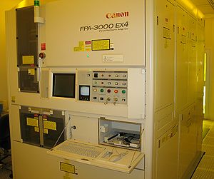
The deep-UV stepper FPA-3000EX4 from Canon is an advanced exposure system designed for mass-production of 6 and 8 inch wafers/ devices having a throughput of up to 90 wafers per hour. The largest applicable thickness of the wafers/ devices is 1,2 mm. Also 4" wafers/ devices can be processed with some restrictions concerning throughput, resolution, uniformity and maximum allowed wafer thickness. The system is equipped with a KrF Excimer laser from Cymer (wavelength 248 nm). Its projection lens’ NA is variable over a range between 0,4 and 0,6. Additionally, the partial coherence factor (σ) of the illumination system can be adjusted and different off-axis illumination modes can be selected.
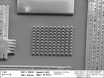
The critical dimension (CD) of patterns that can be realized is specified at around 250nm for arbitrary formed patterns in the standard illumination mode (NA=0,6; σ =0,65). However, the best achievable resolution is different for each pattern type, pattern shape and pitch. So linewidths down to 160 nm could be achieved for geometrically simple patterns or pattern arrays (single and multiple line or pin-hole structures).
The user manual(s), quality control procedure(s) and results and contact information can be found in LabManager.
Process information
| Purpose |
Exposure system designed for mass/production of devices with linewidth down to 250nm | ||
|---|---|---|---|
| Specifications | Magnification |
1:5 | |
| Projection lens Numerical Aperture |
0,4 - 0,60 | ||
| Illumination system's σ |
0,2 - 0,75 (standard illumination mode: σ = 0,65) | ||
| Exposure source |
KrF laser | ||
| Wavelength |
248nm | ||
| Illumination intensity |
2800 W/m2 | ||
| Illumination uniformity |
1,2% | ||
| Maximum printed field size |
22 x 26 mm (maximum on wafer) | ||
| Alignment accuracy |
3 sigma = 50 nm | ||
| Substrates | Substrate size |
| |
| Allowed materials |
| ||
| Batch |
1 - 25 | ||
The content on this page, including all images and pictures, was created by DTU Nanolab staff, unless otherwise stated.
Developer: TMAH UV-lithography

Tool description
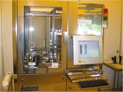
This developer is dedicated for development of DUV resists. The developer is fully automatic and can run 1-25 substrates in a single batch. Supported substrate sizes are 100 mm, 150 mm and 200 mm (200 mm requires tool change).
The machine is equipped with 1 developer line with 2,38% TMAH in water (AZ 726 MIF), 1 topside rinse line with DI water, 1 backside rinse line with DI water and 1 Nitrogen line for drying.
The developer dispense, puddle time, agitation, rinse and drying is controlled by the tool.
| Product: | Süss MicroTec Gamma 2M developer |
|---|---|
| Year of purchase: | 2013 |
| Location: | Cleanroom F-3 |
User manual
The user manual and contact information can be found in LabManager - requires login
Tool training
Training on the tool requires users to complete the lithography TPT followed by the online tool training and a hands-on authorization training.
The tool training video is part of the online tool training, but can also be viewed here.
| Tool purpose |
Development of DUV resists:
May also be used for development of:
|
|---|---|
| Developer | AZ 726 MIF (2.38% TMAH) |
| Development method | Puddle |
| Handling method |
|
| Process temperature | Room temperature |
| Process agitation | 1 cycles per 30 seconds |
| Process rinse | DI water |
| Substrate sizes |
|
| Substrate materials |
|
| Substrate batch size | 1-25 |
| Media flow rates |
|
Process information

Processing on Developer TMAH stepper consists of the following steps:
- Post-exposure bake
- Puddle development
- Rinse
Features of Developer TMAH stepper:
- Cassette-to-cassette wafer handling
- In-line hotplates
- In-line cool plate
- Puddle developer module with rinse and dry
The development process will be performed by the customer together with the Lithography group of DTU Nanolab. In case you would like to do DUV lithography please contact Lithography team, who will consult you and run your wafers together with you.
Here you can find a chart demonstrating a dependence between 250 nm line width/pillars diameter and exposure dose.
Post-exposure baking
Chemically amplified resists and cross-linking negative resists must be baked after exposure in order to finish the process initiated by the exposure light. Post-exposure bake, or PEB, is carried out on one of the two hotplates. After baking, the wafer is cooled for 20 seconds on the 20°C cool plate.
Puddle Development
Development on Developer TMAH stepper is divided into the following steps:
- Pre-wet
- Puddle dispense
- Development
- Spin-off
Pre-wet may be done using developer or DI water, or it may be skipped. It consists of a short dispense at medium spin speed (2s @ 1200 rpm).
Puddle dispense is done by dispensing developer (AZ 726 MIF) to the center of the wafer in order to build up a puddle of developer on the wafer. During the dispense, the wafer may be stopped or rotating slowly (30 rpm). The developer is dispensed at a rate of approximately 500 ml/min.
Development is carried out by leaving the developer puddle on the wafer for the duration of the development time (puddle time). The rotation is stopped during the development, but the developer may be agitated by rotating the wafer a few turns at low speed, e.g. 2s @ 30 rpm halfway through the development time, in order to facilitate good uniformity.
Spin-off is designed to stop the development by removing the developer from the wafer before the rinse. It is usually carried out as a short spin at high speed (3s @ 4000 rpm), but may be omitted.
Processes are divided into single puddle (SP), double puddle (DP), and multiple puddle (MP).
Rinse
After development, the substrate is rinsed using DI water, and dried using nitrogen.
The standard rinse and dry procedure is 30s at 4000 rpm with DIW being administered from the top at the center of the substrate, followed by a 10-15s dry at 3000 rpm using nitrogen from the top at the center of the substrate. The top side rinse is at a rate of approximately 350 ml/min. The flow rate of the nitrogen is 50 l/min, and the drying time is set according to the size of the substrate.
Standard Processes
NB: The list of standard processes is not necessarily complete, as new processes are added over time.
Development (only)
Development sequences on Developer TMAH stepper are divided into the following steps: Pre-wet, puddle dispense, development, spin-off, and finally rinse and dry.
Single puddle:
- 1004 DCH DEV 60s
- 1104 DCH 100mm SP 60s
- 1105 DCH 150mm SP 60s
- 1106 DCH 200mm SP 60s
Post-exposure baking (only)
Chemically amplified resists and cross-linking negative resists must be baked after exposure (Post-Exposure Bake, PEB) in order to finish the process initiated by the exposure light:
- (1000) DCH PEB 130C 60s
- (1001) DCH PEB 130C 90s
The baking is done at 130°C followed by a cooling step at 20°C for 20 seconds.
Combined PEB and development
For convenience, the PEB and development function of the machine may be combined in one sequence:
- (1002) DCH PEB_60s and DEV_60s
- (1003) DCH PEB_90s and DEV_60s
