Specific Process Knowledge/Lithography/UVLithography
Appearance
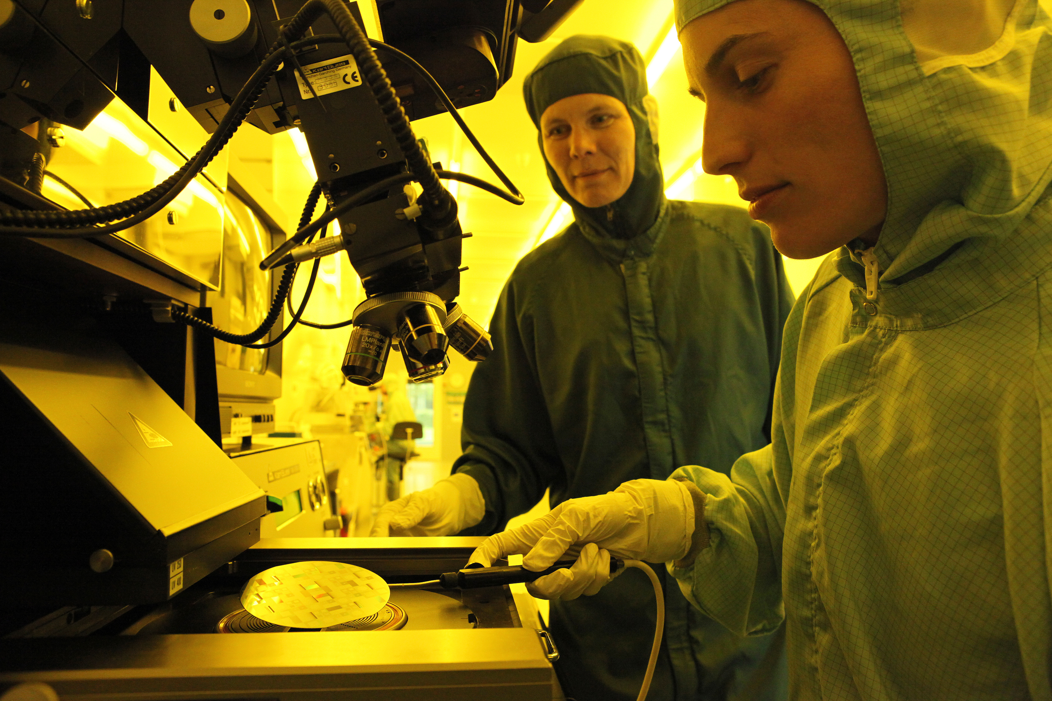
UV Lithography uses ultraviolet light to transfer a pattern from a mask to a wafer coated with photoresist. The photoresist film is spin coated on the wafers and the pattern is transferred to the wafer by using a mask aligner. DTU Danchip houses a number of automatic or semi-automatic coaters and mask aligners.

Resist Overview
| Resist | Polarity | Manufacturer | Comments | Technical reports | Spin Coating | Developer | Rinse | Remover | Process flows (in docx-format) |
| AZ5214E | Positive | AZ Electronic Materials | Can be used for both positive and reverse processes with resist thickness between 1 to 4um. | AZ5214E.pdf | SSE, KS Spinner, III-V Spinner | 351B developer | DI water | Acetone | |
| AZ4562 | Positive | AZ Electronic Materials | For process with resist thickness between 6 and 25um. | AZ4500.pdf | SSE, KS Spinner | 351B developer | DI water | Acetone | Process_Flow_thick_AZ4562_vers2.docx |
| AZ MiR 701 | Positive | AZ Electronic Materials | High selectivity for dry etch. | AZ_MiR_701.pdf | Spin Track 1 + 2 | AZ 726 MIF developer | DI water | Remover 1165 | Process_Flow_AZ_MiR701.docx |
| AZ nLOF 2020 | Negative | AZ Electronic Materials | AZ_nLOF_2020.pdf | Spin Track 1 + 2 | AZ 726 MIF developer | DI water | Remover 1165 | Process_Flow_AZ_nLOF_2020.docx
| |
| SU8 | Negative | Microchem | SU-8_DataSheet_2005.pdf, SU-8_DataSheet_2075.pdf | KS Spinner | PGMEA, Mr60 developer | IPA | Plasma ashing can remove crosslinked SU8. | Process_Flow_SU8_70um.docx
|
