Specific Process Knowledge/Lithography/UVExposure
The contents on this page, including all images and pictures, was created by DTU Nanolab staff unless otherwise stated.
Feedback to this page: click here
UV Exposure Comparison Table
| Equipment | KS Aligner | Aligner: MA6 - 2 | Aligner: Maskless 01 | Aligner: Maskless 02 | Aligner: Maskless 03 | |
|---|---|---|---|---|---|---|
| Purpose |
|
|
|
|
| |
| Performance | Minimum feature size |
~1 µm |
~1 µm |
~1 µm |
~1 µm |
~1 µm |
| Exposure light/filters/spectrum |
|
|
365nm LED |
375nm laserdiodes |
405nm laserdiodes | |
| Exposure mode |
|
|
|
|
| |
| Substrates | Batch size |
|
|
|
|
|
| Allowed materials |
|
|
|
|
| |
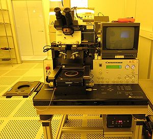
KS Aligner
SUSS Mask Aligner MA6 is designed for high resolution photolithography. The 365nm exposure wavelength version is capable of 1.25 (1.0) um resolution in vacuum contact. All contact exposure programs (vacuum, hard, soft, proximity) are supplied. Two alignment options are available: top side alignment (TSA) with a split field or a video microscope and back side alignment (BSA) with BSA microscope. It is also possible to make IR- light alignment.
Training videos:
The user manual(s), quality control procedure(s) and results and contact information can be found in LabManager - requires login
Exposure dose
Information on UV exposure dose
Process information
The KS Aligner has an i-line notch filter installed. This results in an exposure light peak around 365nm with a FWHM of 7nm.
Quality Control (QC)
| Quality Control (QC) for KS Aligner | ||||||||||||||||
Power supply and/or lamp will be adjusted if intensity is outside the limit. |
| Purpose |
Alignment and UV exposure | ||
|---|---|---|---|
| Performance | Exposure mode |
vacuum contact, hard contact, soft contact, proximity, flood exposure | |
| Exposure light/filters |
| ||
| Minimum structure size |
down to 1.25µm | ||
| Mask size |
| ||
| Alignment modes |
| ||
| Substrates | Substrate size |
| |
| Allowed materials |
All cleanroom materials Dedicated chuck for III-V materials | ||
| Batch |
1 | ||
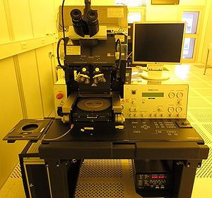
Aligner: MA6 - 2
The Süss MicroTek Mask Aligner MA6 is designed for high resolution photolithography. The 365nm exposure wavelength version is capable of 1.25 (1.0) um resolution in vacuum contact. All contact exposure programs (vacuum, low vacuum, hard, soft, proximity) are supplied. Two alignment options are available: top side alignment (TSA) with a split field or a video microscope and back side alignment (BSA) with BSA (video) microscope.
The aligner can also be used for bond alignment (for Wafer Bonder 02). Special training is required.
Training videos:
The user manual, quality control procedures and results, user APVs, and contact information can be found in LabManager - requires login
Exposure dose
Information on UV exposure dose
Process information
The Aligner: MA6 - 2 has an i-line notch filter installed. This results in an exposure light peak at 365nm. Compared to exposure on the KS Aligner, the optimal dose should be very similar. The 500W Hg-Xe lamp also enables exposure in the DUV range around 240nm. This functionality is not established yet, partly due to safety concerns.
Quality Control (QC)
| Quality Control (QC) for Aligner: MA6-2 | ||||||||||||||||
Power supply and/or lamp will be adjusted if intensity is outside the limit. |
Alignment
Top Side Alignment:
- TSA microscope standard objectives: 5X, and 10X (20X available)
- TSA microscope special objectives: 11.25X offset (for smaller separation)
- Minimum distance between TSA microscope objectives: 33 mm (8 mm for special objectives)
- Maximum distance between TSA microscope objectives: 160 mm
- TSA microscope travel range: X +/- 25mm; Y +20mm / -75mm (towards flat)
BackSide Alignment:
- Minimum distance between BSA microscope objectives: 15 mm
- Maximum distance between BSA microscope objectives: 100 mm
- BSA microscope travel range: X +50mm / -16mm; Y +50mm / -20mm (towards flat)
- BSA chuck view ranges:
- 2": X +/- 8-22mm; Y +/- 0-6mm
- 4": X +/- 14-46mm; Y +/- 0-10mm
- 6": X +/- 14-69mm; Y +/- 0-10mm
Microscope field of view (W x H, splitfield):
- TSA 5X
- Oculars: 1.3mm x 2.6mm (Ø2.6mm full field)
- Camera: 350µm x 500µm (700µm x 500µm full field)
- TSA 10X
- Oculars: 0.6mm x 1.3mm (Ø1.3mm full field)
- Camera: 150µm x 250µm (350µm x 250µm full field)
- TSA special
- Oculars: 0.55mm x 1.1mm (Ø1.1mm full field)
- Camera: 150µm x 200µm (300µm x 200µm full field)
- BSA camera
- Low: 1.5mm x 2mm (3mm x 2mm full field)
- High: 450µm x 650µm (950µm x 650µm full field)
| Purpose |
Mask alignment and UV exposure, potentially DUV exposure 1) Bond alignment | ||
|---|---|---|---|
| Performance | Exposure mode |
vacuum contact, hard contact, soft contact, proximity, flood exposure | |
| Exposure light/filters |
| ||
| Minimum structure size |
Typically 1.25 µm, possibly down to 0.8 µm 1) | ||
| Mask size |
| ||
| Alignment modes |
| ||
| Substrates | Substrate size |
| |
| Allowed materials |
All cleanroom materials except copper and steel Dedicated chuck for III-V materials | ||
| Batch |
1 | ||
1) Not available yet. Requires tool change. Would require safety investigation (and a dedicated project) to become available.
Aligner: Maskless 01
The logon password for the PC is "mla" (without quotation marks).
The MLA 100 Maskless Aligner located in the E-4 cleanroom is a direct exposure lithography tool installed in 2017. It is a UV LED exposure system, that exposes the patterns directly on photosensitive resists on chips, 2, 4, and 6 inch substrates, without prior fabrication of the mask. The system offers top side alignment with high accuracy.
The user manual and contact information can be found in LabManager:
Equipment info in LabManager - requires login
Exposure dose and defocus
Information on UV exposure dose
Process information
- Exposure technology
- Process parameters
- Substrate positioning
- Alignment
- Optimal use of the maskless aligner
| Purpose |
Alignment and UV exposure | ||
|---|---|---|---|
| Performance | Exposure mode |
Projection | |
| Exposure light |
365nm (LED), FWHM=8nm | ||
| Focusing method |
Pneumatic | ||
| Minimum structure size |
down to 1µm | ||
| Design formats |
| ||
| Alignment modes |
Top side only | ||
| Substrates | Substrate size |
| |
| Allowed materials |
All cleanroom materials | ||
| Batch |
1 | ||
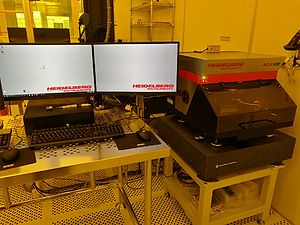
Aligner: Maskless 02
MLA150 WMII maskless aligner from Heidelberg Instruments GmbH (installed 2019 as WMI (0.6µm resolution), rebuilt to WMII 2023).
Special features
- Optical Autofocus
- Backside Alignment
- Basic Gray Scale Exposure
- Advanced Field Alignment Mode for alignment to individual chips/devices on the substrate
- High Aspect Ratio Mode for exposure of thick resists
- 200 x 200 mm exposure field
- Separate conversion PC
Equipment info in LabManager - requires login
Exposure dose and defocus
Information on UV exposure dose
Process information
| Purpose |
Alignment and UV exposure | ||
|---|---|---|---|
| Performance | Exposure mode |
Projection | |
| Exposure light |
(laser diode arrays) | ||
| Focusing method |
| ||
| Minimum structure size |
down to 1 µm | ||
| Design formats |
| ||
| Alignment modes |
| ||
| Substrates | Substrate size |
| |
| Allowed materials |
All cleanroom materials | ||
| Batch |
1 | ||
1) with optical autofocus
Aligner: Maskless 03
MLA150 WMII maskless aligner from Heidelberg Instruments GmbH, installed 2020.
Special features:
- Backside Alignment
- Advanced Field Alignment Mode for alignment to individual chips/devices on the substrate
- Separate conversion PC (Power PC)
Equipment info in LabManager - requires login
Exposure dose and defocus
Information on UV exposure dose
Process information
| Purpose |
Alignment and UV exposure | ||
|---|---|---|---|
| Performance | Exposure mode |
Projection | |
| Exposure light |
405nm | ||
| Focusing method |
Pneumatic | ||
| Minimum structure size |
down to 1 µm | ||
| Design formats |
| ||
| Alignment modes |
| ||
| Substrates | Substrate size |
| |
| Allowed materials |
All cleanroom materials | ||
| Batch |
1 | ||


