Specific Process Knowledge/Lithography/Development
The contents on this page, including all images and pictures, was created by DTU Nanolab staff unless otherwise stated.
Feedback to this page: click here
Development Comparison Table
| Equipment | Developer: SU8 (Wet bench) | Developer: E-beam | Developer: TMAH Manual | Developer: TMAH UV-lithography | Developer: TMAH Stepper | |
|---|---|---|---|---|---|---|
| Purpose |
|
Development of:
|
Development of:
|
Development of:
|
Development of:
Post-exposure baking |
Development of:
Post-exposure baking |
| Developer |
mr-Dev 600 (PGMEA) |
|
AZ 726 MIF (2.38% TMAH in water) |
AZ 726 MIF (2.38% TMAH in water) |
AZ 726 MIF (2.38% TMAH in water) | |
| Method | Development |
Submersion |
Spray/Puddle |
Puddle |
Puddle |
Puddle |
| Handling |
|
|
|
Vacuum chuck |
Vacuum chuck | |
| Process parameters | Temperature |
Room temperature |
Room temperature |
Room temperature |
Room temperature |
Room temperature |
| Agitation |
Magnetic stirrer |
Rotation |
Rotation |
Rotation |
Rotation | |
| Rinse |
IPA |
IPA |
DI water |
DI water |
DI water | |
| Substrates | Substrate size |
|
|
|
|
|
| Allowed materials |
|
All cleanroom approved materials |
|
|
| |
| Batch |
1 - 6 |
1 |
1 |
1 - 25 |
1 - 25 | |
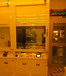
Developer: SU8 (Wet Bench)
The SU8-Developer bench is a manually operated wet bench for submersion development of SU-8 photoresist in PGMEA (supplied in the cleanroom as mr-Dev 600). The development process is in two stages; one bath (FIRST) to dissolve the bulk of the resist, and a second, cleaner bath (FINAL) to finish the development. The development time is controlled manually by the user. After development, the substrates are rinsed with IPA in dedicated IPA bath and put for drying in the empty bath.
The user manual, user APV, and contact information can be found in LabManager: Developer: SU8(Wet Bench) - requires login
Process information
Several aspects of the outcome of SU-8 processing are affected by the development process. The lithographic resolution is affected by the time between PEB (post-exposure bake) and development, as the cross-linking process continues in the interface between exposed and unexposed regions even at room temperature. Cracks in the structures is affected by two things; the development time, and how much has previously been developed in the developer bath. Cracking is worse with longer development time, and worst in a new developer bath. The effect of the developer use quickly saturates (5-10 wafers). Finally, the stability of fine structures (high aspect ratio) is affected by the rinse after development, as the lower surface tension of IPA compared to PGMEA reduces pattern collapse during drying.
Development time is strongly dependent on the SU-8 thickness.
- Minimum development time: 1 min per 20 µm in FIRST
Suggestions:
- 2-5µm: 2 min. in FIRST; 2 min. in FINAL
- 40µm: 5 min. in FIRST; 5 min. in FINAL (however, 3 min. in FIRST and 2 min. in FINAL is sufficient)
- 180-250µm: 15 min. in FIRST; 15 min. in FINAL
| Purpose |
Development of:
| |
|---|---|---|
| Developer |
mr-Dev 600 (PGMEA) | |
| Method | Development |
Submersion |
| Handling |
Single wafer holder | |
| Process parameters | Temperature |
Room temperature |
| Agitation |
Magnetic stirrer | |
| Rinse |
IPA | |
| Substrates | Substrate size |
|
| Allowed materials |
| |
| Batch |
1-6 |
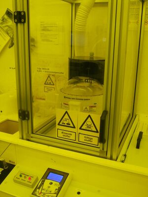
Developer: E-beam
Developer: E-beam is a manually operated, single substrate or chip spray-puddle developer. It uses the N50 or AR 600-546 developers and IPA for rinsing. The substrates or chips are loaded manually one by one into the developer. Developer dispense, puddle time, IPA rinse, and drying is performed automatically by the equipment.
The machine is setup to agitate and be stationary to enhance the development uniformity - this is a ongoing process.
Training video (for Developer: TMAH Manual, but it is the same model)
The user manual, user APV, and contact information can be found in LabManager - requires login
Process information
All recipes are single puddle. N50 and 546 denotes the developer used (546 is short for AR 600- 546). The first step is pressurizing the canister so nothing will happen visually. Please watch if the developer and rinsing starts. If not try to restart the machine by pressing the EMO and turning it on again. The spray is 8-10 s and will start the development process hence the short recipes (10s and 30s.) have been adjusted according to this.
Process recipes
- 546 10s: 10s. Development Rinse and dry.
- 546 30s: 60s. Development Rinse and dry.
- 546 60s: 60s. Development Rinse and dry.
- 546 180s: 180s. Development Rinse and dry.
- N50 10s: 10s. Development Rinse and dry.
- N50 30s: 30s. Development Rinse and dry.
- N50 60s: 60s. Development Rinse and dry.
- N50 90s: 90s. Development Rinse and dry.
- N50 120s: 120s. Development Rinse and dry.
- N50 180s: 180s. Development Rinse and dry.
- N50 300s: 300s. Development Rinse and dry.
- N50 180s6": Test for changing the agitation for 6" uniformity 180s. Development Rinse and dry.
- Testdev: The time can be modified 60s. Development Rinse and dry on AR 600-546.
- Rinse: Rinse and dry.
Utility recipes
- UTIL-DR: Dome rinse.
- UTIL-BE: Bottle empty. Nanolab use only.
| Purpose |
Development of:
| |
|---|---|---|
| Developer |
| |
| Method | Development |
Spray/Puddle |
| Handling |
| |
| Process parameters | Temperature |
Room temperature |
| Agitation |
Rotational agitation at 15 rpm | |
| Rinse |
IPA | |
| Substrates | Substrate size |
|
| Allowed materials |
| |
| Batch |
1 |
Developer: TMAH Manual
Developer: TMAH Manual is a manually operated, single substrate or chip puddle developer. It uses the TMAH based AZ 726 MIF developer (2.38 % TMAH in water with a small amount of wetting agent). The substrates or chips are loaded manually one by one into the developer. Developer dispense, puddle time, water rinse, and drying is performed automatically by the equipment.
The user manual, user APV, and contact information can be found in LabManager - requires login
Process information
All recipes use the following structure:
- Pressurize the TMAH canister
- Dispense puddle while rotating substrate slowly
- Puddle development while not rotating
- Agitate substrate once per 30 seconds by rotating slowly for 1 second
- Spin off developer
- Clean substrate and chamber with DI water
- Dry substrate and chamber with nitrogen
Multi-puddle recipes repeat steps 2-5 for the given number of puddles.
Process recipes
SP: Single-puddle
MP: Multi-puddle
- 1 Rinse
- 2 SP 15s
- 3 SP 30s
- 4 SP 60s
- 5 SP 90s
- 6 SP 120s
- 7 MP 2x60 s
- 8 MP 4x60 s
- 9 MP 6x60 s
| Purpose |
Development of UV resists:
Development of DUV resists:
| |
|---|---|---|
| Developer |
AZ 726 MIF (2.38% TMAH in water) | |
| Method | Development |
Puddle |
| Handling |
| |
| Process parameters | Temperature |
Room temperature |
| Agitation |
1 per 30 seconds: | |
| Rinse |
DI water | |
| Substrates | Substrate size |
|
| Allowed materials |
| |
| Batch size |
1 |
Developer TMAH UV-lithography
Developer TMAH UV-lithography was released Q4 2014.
The user manual, user APV, and contact information can be found in LabManager - requires login
Process Information
| Purpose |
Development of
| |
|---|---|---|
| Developer |
AZ 726 MIF (2.38% TMAH in water) | |
| Method | Development |
Puddle |
| Handling |
Vacuum chuck | |
| Process parameters | Temperature |
Room temperature |
| Agitation |
Rotation | |
| Rinse |
DI water | |
| Substrates | Substrate size |
|
| Allowed materials |
Silicon and glass substrates Film or pattern of all except Type IV | |
| Batch |
1-25 |
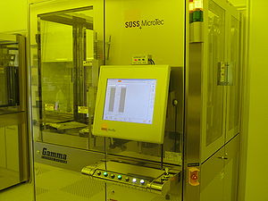
Developer: TMAH Stepper
This developer is dedicated for development of DUV resists. The developer is fully automatic and can run up to 25 substrates in a batch 4", 6", and 8" size (8" requires tool change). The machine is equipped with 1 developer line, in our case 2,38% TMAH in water (AZ 726 MIF), 1 topside rinse line with water, 1 backside rinse line with water and 1 N2 line for drying.
The user manual and contact information can be found in LabManager - requires login
Process information
The development process will be performed by the customer together with the Photolith group of DTU Nanolab. In case you would like to do DUV lithography please contact Lithography team, who will consult you and run your wafers together with you.
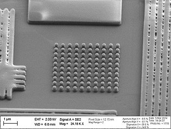
Here you can find a chart demonstrating a dependence between 250 nm line width/pillars diameter and exposure dose.
Standard processes
Post-exposure bake sequences:
- (1000) DCH PEB 130C 60s 60s baking at 130°C; 20s cooling
- (1001) DCH PEB 130C 90s 90s baking at 130°C; 20s cooling
Development sequences:
- (1004) DCH DEV 60s 60s single puddle development
Combined PEB and development sequences:
- (1002) DCH PEB_60s and DEV_60s 60s baking at 130°C followed by 60s single puddle development
- (1003) DCH PEB_90s and DEV_60s 90s baking at 130°C followed by 60s single puddle development
The standard developer process consists of:
- pre-wetting with water (2.5s @ 1000rpm)
- developer dispense (2.5s @ 40rpm, corresponding to ~9ml)
- development (60s @ 0rpm)
- water rinse with BSR (5s @ 3000rpm)
- nitrogen drying (7s @ 4000rpm)
and has a cycle time of ~2 minutes
| Purpose |
Development of DUV resist: KRF M230Y and KRF M35G | ||
|---|---|---|---|
| Developer |
2,38% water based TMAH | ||
| Process parameters | Spin speed |
10 - 5000 rpm | |
| Spin acceleration |
100 - 10000 rpm/s | ||
| Hotplate temperature |
130°C for post exposure baking | ||
| Substrates | Substrate size |
| |
| Allowed materials |
| ||
| Batch |
1 - 25 | ||


