Specific Process Knowledge/Lithography/UVLithography: Difference between revisions
| Line 204: | Line 204: | ||
==[[Specific Process Knowledge/Lithography/Coaters|Coaters]]== | ==[[Specific Process Knowledge/Lithography/Coaters|Coaters]]== | ||
==[[Specific Process Knowledge/Lithography/UVExposure|UV Exposure]]== | ==[[Specific Process Knowledge/Lithography/UVExposure|UV Exposure]]== | ||
==[[Specific_Process_Knowledge/Lithography/UVExposure_Dose|Information on UV Exposure Dose]]== | ===[[Specific_Process_Knowledge/Lithography/UVExposure_Dose|Information on UV Exposure Dose]]=== | ||
==[[Specific Process Knowledge/Lithography/Baking|Baking]]== | ==[[Specific Process Knowledge/Lithography/Baking|Baking]]== | ||
==[[Specific Process Knowledge/Lithography/Development|Development]]== | ==[[Specific Process Knowledge/Lithography/Development|Development]]== | ||
Revision as of 14:07, 19 March 2020
Feedback to this page: click here

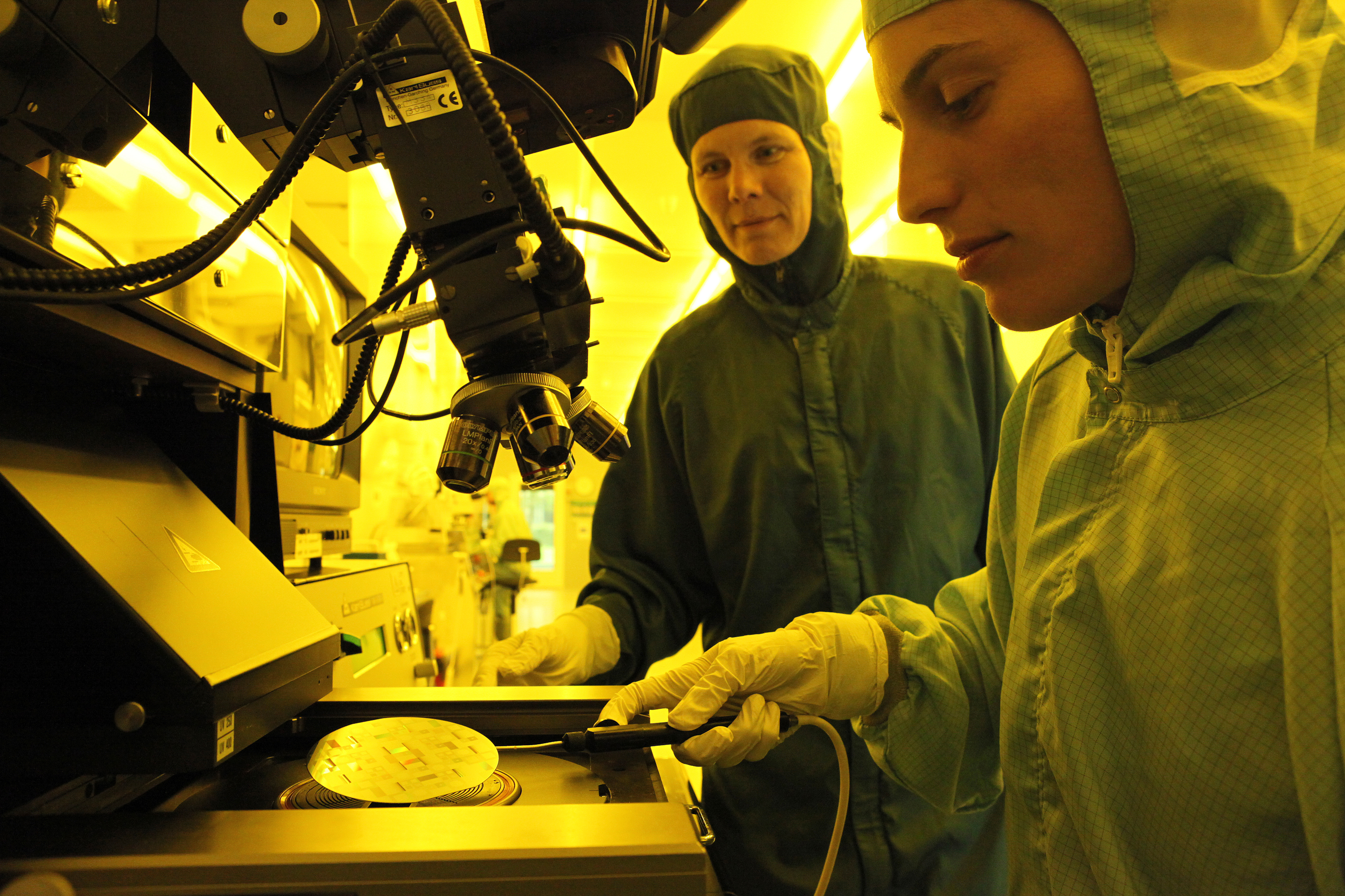
UV Lithography uses ultraviolet light to transfer a pattern from a mask to a wafer coated with photoresist. The photoresist film is spin coated on the wafers and the pattern is transferred to the wafer by using a mask aligner. DTU Nanolab houses a number of automatic or semi-automatic coaters and mask aligners.
Getting started


Before you plan your UV processing and request for training on any equipment in UV lithography, please go through the following steps. Include the information in the training request.
If you are new to photolithography, you can visit this wikipedia webpage about photolithography before you start.
- Prepare a process flow which describes all steps in your UV lithography process. You can find docx-templates in this table.
- Substrate pretreatment: In many processes it is recommended to pretreat or prime your wafer before spin-coating. In some spin-coaters, these pretreatment processes are included in the spin coating of resist.
- Spin Coater: Do you wish to use a manual spin coater or a robot spin coater? See a list of spin coaters here.
- Resist Type: Choose the type of resist you wish to use: a list of UV lithography resist types available at DTU Nanolab can be found on this page.
- Positive tone resist: Resist exposed to UV light will be dissolved in the developer. The mask openings are an exact copy of the resist pattern which is to remain on the wafer.
- Negative tone resist: Resist exposed to UV light will become polymerized and difficult to dissolve. The mask openings are an inverse copy of the resist pattern which is to remain on the wafer.
- Thickness of resist: In general, it is recommended to work at or below an aspect ratio of ~1, i.e. where the width of the pattern is larger than the thickness of the resist. Furthermore, when you decide for the resist thickness, consider which transfer you need:
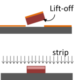
- For lift-off processes, we recommend resist thickness at least 5 times larger than the thickness of the metal to be lifted.
- For dry etch or wet etch processes, investigate the resist etch rate of your process as this might limit the minimum thickness of your resist.
- Exposure: Choose which aligner you wish to use, and consider the exposure dose.
- Mask: Design and order a photomask for your UV process. A detailed instruction on how to design and order a photomask can be found here.
- Development: Choose which equipment you wish to use to develop your photoresist from this list. Remember the development process influences the exposure dose.
Resist Overview
| Resist | Polarity | Spectral sensitivity | Manufacturer | Comments | Technical reports | Spin Coating | Exposure | Developer | Rinse | Remover | Process flows (in docx-format) |
| AZ 5214E | Positive but the image can be reversed | 310 - 420 nm | Merck KGaA
Supplied by MicroChemicals GmbH |
Can be used for both positive and image reversed (negative) processes with resist thickness between 1 and 4 µm. | AZ5214E.pdf | Automatic spin coater (Gamma UV or Gamma e-beam & UV) | Mask aligner (KS or MA6 - 2) | AZ 351B developer
or |
DI water | Acetone | |
| AZ 4562 | Positive | 310 - 440 nm | Merck KGaA
Supplied by MicroChemicals GmbH |
For process with resist thickness between 6 and 25 µm. | AZ4500.pdf | Automatic spin coater (Gamma e-beam & UV) | Mask aligner (KS or MA6 - 2) | AZ 351B developer
or |
DI water | Acetone | Process_Flow_thick_AZ4562.docx |
| AZ MiR 701 | Positive | 310 - 445 nm | Merck KGaA
Supplied by MicroChemicals GmbH |
High selectivity for dry etch.
Resist thickness 1.5 - 4 µm. |
AZ_MiR_701.pdf | Automatic spin coater (Gamma UV or Gamma e-beam & UV) | Mask aligner (KS or MA6 - 2) | AZ 726 MIF developer | DI water | Remover 1165 | Process_Flow_AZ_MiR701.docx |
| AZ nLOF 2020 | Negative | 310 - 380 nm | Merck KGaA
Supplied by MicroChemicals GmbH |
Negative sidewalls for lift-off.
Resist thickness 1.5 - 4 µm. |
AZ_nLOF_2020.pdf | Automatic spin coater (Gamma UV) | Mask aligner (KS or MA6 - 2) | AZ 726 MIF developer | DI water | Remover 1165 | Process_Flow_AZ_nLOF_2020.docx |
| SU-8 | Negative | 350 - 400 nm | Kayaku Advanced Materials, Inc.
Supplied by micro resist technology GmbH |
High aspect ratio.
Resist thickness 1 µm to several 100 µm. |
SU-8_DataSheet_2005.pdf, SU-8_DataSheet_2075.pdf | Manual spin coater (LabSpin or RCD8) | Mask aligner (KS or MA6 - 2) | mr-Dev 600 developer (PGMEA) | IPA | Plasma ashing can remove crosslinked SU-8 | Process_Flow_SU8_70um.docx |
Process information
Information from our suppliers
Application notes from Microchemicals GmbH, e.g. Lithography Trouble-Shooter
