Specific Process Knowledge/Lithography/UVLithography: Difference between revisions
| Line 157: | Line 157: | ||
=Process information= | =Process information= | ||
==[[Specific_Process_Knowledge/Lithography/UVLithography#Resist_Overview|UV Resist Overview]]== | |||
*[[Specific Process Knowledge/Lithography/Pretreatment|Pretreatment]] | *[[Specific Process Knowledge/Lithography/Pretreatment|Pretreatment]] | ||
*[[Specific Process Knowledge/Lithography/Coaters|Coaters]] | *[[Specific Process Knowledge/Lithography/Coaters|Coaters]] | ||
Revision as of 15:06, 24 November 2014
Feedback to this page: click here

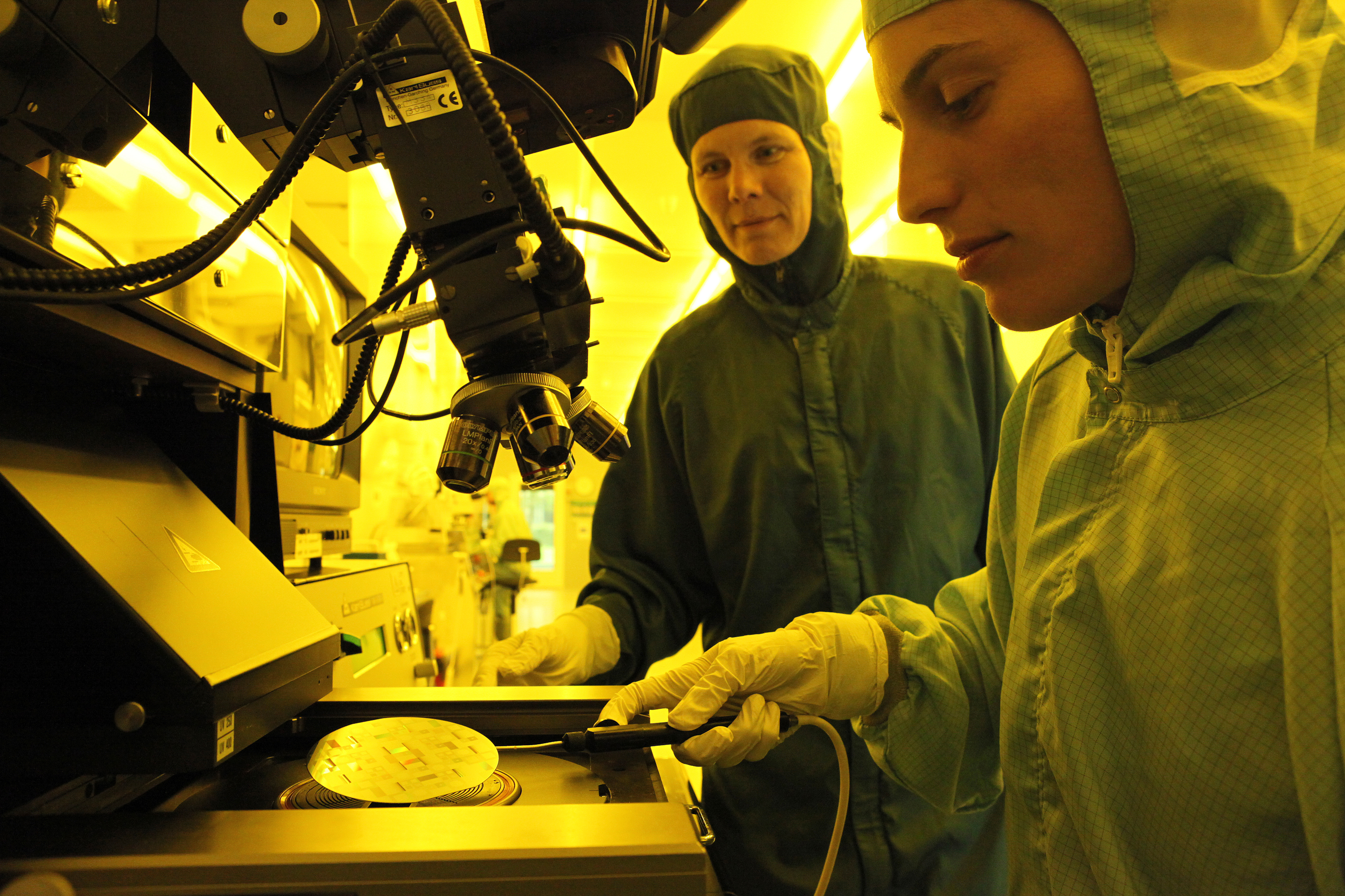
UV Lithography uses ultraviolet light to transfer a pattern from a mask to a wafer coated with photoresist. The photoresist film is spin coated on the wafers and the pattern is transferred to the wafer by using a mask aligner. DTU Danchip houses a number of automatic or semi-automatic coaters and mask aligners.
Mask Design
In order to realize your device you will need a way to draw the patterns that define the structures in the different layers on the wafer. This is done in a drawing tool for mask layout. The output is a file you send to a mask house, which in return supplies you with a number of photolithographic masks. Each mask is a glass plate with a chromium pattern that mimics a layer in your layout.
Please read more details here: Mask Design
Resist Overview
| Resist | Polarity | Spectral sensitivity | Manufacturer | Comments | Technical reports | Spin Coating | Exposure | Developer | Rinse | Remover | Process flows (in docx-format) |
| AZ 5214E | Positive but the image can be reversed | 310 - 420 nm | AZ Electronic Materials | Can be used for both positive and reverse processes with resist thickness between 1 and 4 µm. | AZ5214E.pdf | SSE,
KS Spinner or |
KS Aligner, | AZ 351B developer
or |
DI water | Acetone | |
| AZ 4562 | Positive | 310 - 440 nm | AZ Electronic Materials | For process with resist thickness between 6 and 25 µm. | AZ4500.pdf | SSE or | KS Aligner, | AZ 351B developer
or |
DI water | Acetone | Process_Flow_thick_AZ4562.docx |
| AZ MiR 701 | Positive | 310 - 445 nm | AZ Electronic Materials | High selectivity for dry etch.
Resist thickness 1 - 2 µm. |
AZ_MiR_701.pdf | Spin Track 1 + 2 | KS Aligner, | AZ 726 MIF developer | DI water | Remover 1165 | Process_Flow_AZ_MiR701.docx |
| AZ nLOF 2020 | Negative | 310 - 380 nm | AZ Electronic Materials | Negative sidewalls for lift-off.
Resist thickness 1.5 - 3 µm. |
AZ_nLOF_2020.pdf | Spin Track 1 + 2 | KS Aligner, | AZ 726 MIF developer | DI water | Remover 1165 | Process_Flow_AZ_nLOF_2020.docx |
| SU-8 | Negative | 350 - 400 nm | Microchem | High aspect ratio.
Resist thickness 1 µm to several 100 µm. |
SU-8_DataSheet_2005.pdf, SU-8_DataSheet_2075.pdf | KS Spinner | Aligner-6inch,
KS Aligner or |
mr-Dev 600 developer (PGMEA) | IPA | Plasma ashing can remove crosslinked SU-8 | Process_Flow_SU8_70um.docx |
Process information
UV Resist Overview
- Pretreatment
- Coaters
- UV Exposure
- Information on UV Exposure Dose
- Baking
- Development
- Striping Resist
- Lift-off
