Specific Process Knowledge/Lithography/UVLithography: Difference between revisions
Appearance
| Line 19: | Line 19: | ||
#* For [[Specific_Process_Knowledge/Lithography/LiftOff|lift-off]] processes, we recommend resist thicknnesses ~5 times larger than the thickness of the metal to be lifted. | #* For [[Specific_Process_Knowledge/Lithography/LiftOff|lift-off]] processes, we recommend resist thicknnesses ~5 times larger than the thickness of the metal to be lifted. | ||
#* For dry or wet etch processes, investigate the resist etch rate of your process as this might limit the minimum thickness of your resist. | #* For dry or wet etch processes, investigate the resist etch rate of your process as this might limit the minimum thickness of your resist. | ||
<br><br> | |||
# '''Mask''': Design and order a photomask for your UV process. A detailed instruction on how to design and order a photomask can be found [[Specific_Process_Knowledge/Lithography/Pattern_Design_and_Mask_Fabrication|here]]. | # '''Mask''': Design and order a photomask for your UV process. A detailed instruction on how to design and order a photomask can be found [[Specific_Process_Knowledge/Lithography/Pattern_Design_and_Mask_Fabrication|here]]. | ||
<br> | |||
# '''Substrate pretreatment''': In many processes it is recommended to [[Specific_Process_Knowledge/Lithography/Pretreatment|pretreat]] your wafer before spin-coating. In some spin-coaters, these pretreatment processes are included in the spin coating of resist. If you use either the '''RCD8, SSE or a manual spin coater''', you should book equipment for pretreatment prior to spin coating. | # '''Substrate pretreatment''': In many processes it is recommended to [[Specific_Process_Knowledge/Lithography/Pretreatment|pretreat]] your wafer before spin-coating. In some spin-coaters, these pretreatment processes are included in the spin coating of resist. If you use either the '''RCD8, SSE or a manual spin coater''', you should book equipment for pretreatment prior to spin coating. | ||
Revision as of 13:38, 6 July 2015
Feedback to this page: click here

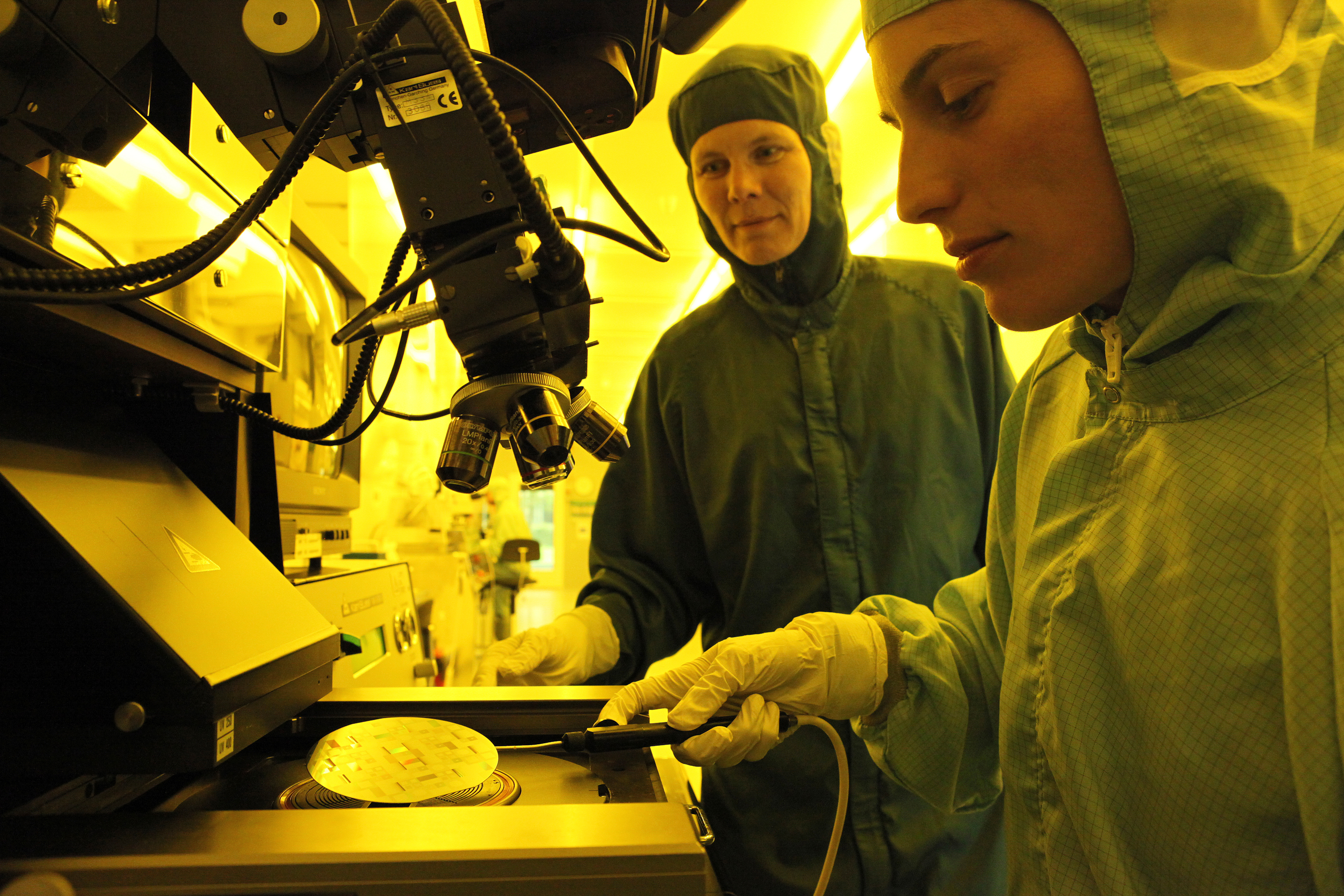
UV Lithography uses ultraviolet light to transfer a pattern from a mask to a wafer coated with photoresist. The photoresist film is spin coated on the wafers and the pattern is transferred to the wafer by using a mask aligner. DTU Danchip houses a number of automatic or semi-automatic coaters and mask aligners.
Getting started
Before you plan your UV processing and request for training on any equipment in UV lithography, go through the following steps:

- Resist Type: Choose the type of resist you wish to use:
- Positive tone resist: Resist exposed to UV light will be dissolved in the developer. The mask is an exact copy of the pattern which is to remain on the wafer.
- Negative tone resist: Resist exposed to UV light will become polymerized and difficult to dissolve. The mask is an inverse copy of the pattern which is to remain on the wafer.
- A list of UV lithography resist types available at DTU Danchip can be found here.
- Thickness of resist: In general, it is recommended to work with an aspect ratio of ~1, i.e. where the width of the pattern is of same size than the thickness of the resist. Furthermore, when you decide for the resist thickness, consider which transfer you need:
- For lift-off processes, we recommend resist thicknnesses ~5 times larger than the thickness of the metal to be lifted.
- For dry or wet etch processes, investigate the resist etch rate of your process as this might limit the minimum thickness of your resist.
- Mask: Design and order a photomask for your UV process. A detailed instruction on how to design and order a photomask can be found here.
- Substrate pretreatment: In many processes it is recommended to pretreat your wafer before spin-coating. In some spin-coaters, these pretreatment processes are included in the spin coating of resist. If you use either the RCD8, SSE or a manual spin coater, you should book equipment for pretreatment prior to spin coating.
Resist Overview
| Resist | Polarity | Spectral sensitivity | Manufacturer | Comments | Technical reports | Spin Coating | Exposure | Developer | Rinse | Remover | Process flows (in docx-format) |
| AZ 5214E | Positive but the image can be reversed | 310 - 420 nm | AZ Electronic Materials | Can be used for both positive and reverse processes with resist thickness between 1 and 4 µm. | AZ5214E.pdf | SSE,
KS Spinner or |
KS Aligner, | AZ 351B developer
or |
DI water | Acetone | |
| AZ 4562 | Positive | 310 - 440 nm | AZ Electronic Materials | For process with resist thickness between 6 and 25 µm. | AZ4500.pdf | SSE or | KS Aligner, | AZ 351B developer
or |
DI water | Acetone | Process_Flow_thick_AZ4562.docx |
| AZ MiR 701 | Positive | 310 - 445 nm | AZ Electronic Materials | High selectivity for dry etch.
Resist thickness 1 - 2 µm. |
AZ_MiR_701.pdf | Spin Track 1 + 2 | KS Aligner, | AZ 726 MIF developer | DI water | Remover 1165 | Process_Flow_AZ_MiR701.docx |
| AZ nLOF 2020 | Negative | 310 - 380 nm | AZ Electronic Materials | Negative sidewalls for lift-off.
Resist thickness 1.5 - 3 µm. |
AZ_nLOF_2020.pdf | Spin Track 1 + 2 | KS Aligner, | AZ 726 MIF developer | DI water | Remover 1165 | Process_Flow_AZ_nLOF_2020.docx |
| SU-8 | Negative | 350 - 400 nm | Microchem | High aspect ratio.
Resist thickness 1 µm to several 100 µm. |
SU-8_DataSheet_2005.pdf, SU-8_DataSheet_2075.pdf | KS Spinner | Aligner-6inch,
KS Aligner or |
mr-Dev 600 developer (PGMEA) | IPA | Plasma ashing can remove crosslinked SU-8 | Process_Flow_SU8_70um.docx |
