Specific Process Knowledge/Lithography/Strip
The content on this page, including all images and pictures, was created by DTU Nanolab staff, unless otherwise stated.
Feedback to this page: click here
Strip Comparison Table
| Plasma Asher 3: Descum | Plasma Asher 4 (Clean) | Plasma Asher 5 (Dirty) | Resist strip | Lift-off | |
|---|---|---|---|---|---|
| Purpose | Resist descum |
|
|
Resist stripping | Metal lift-off |
| Method | Plasma ashing | Plasma ashing | Plasma ashing | Solvent & ultrasonication | Solvent & ultrasonication |
| Process: Gasses | O2 (50 sccm) |
|
|
NA | NA |
| Process: Power | 10-100 W (10-100%) | 150-1000 W | 150-1000 W | NA | NA |
| Process: Solvent | NA | NA | NA |
|
|
| Substrate: Batch |
|
|
|
|
|
| Substrate: Materials |
|
|
|
|
|
Plasma Ashing process parameters
| Photoresist stripping | Descum after lithography | Surface treatment of plastic, ceramic and metal | Ashing of organic material | |
|---|---|---|---|---|
| Process pressure | 1.3 mbar | 1.3 mbar | 0.5-1.5 mbar | 0.5-1.5 mbar |
| Process gases |
|
|
O2, CF4, N2 or their mixtures | O2 |
| Process power | 1000 W | 200 W | 150-1000 W | 1000 W or less for heat- sensitive materials |
| Process time | 5-90 minutes | 1-30 minutes | seconds to minutes | Between 0.5 and 20 hours, depending on the material |
| Batch size | 1-25 | 1-25 | 1 wafer at a time | 1 wafer at a time, use a container, e.g Petri dish |
Plasma Asher 1
Plasma asher 1 was decommissioned 2024-12-02.
Information about decommissioned tool can be found here.
Plasma Asher 2
Plasma asher 2 was decommissioned 2024-12-02.
Information about decommissioned tool can be found here.
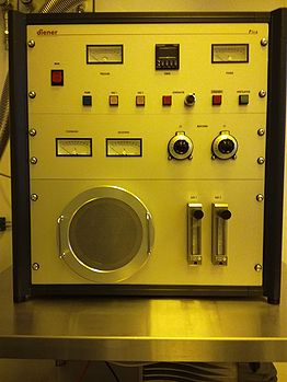
Plasma Asher 3: Descum

Product name: Diener Pico Plasma Asher
Year of purchase: 2014
The Plasma Asher 3: Descum is dedicated for resist descum, i.e. removal of remains resist traces after development. It has a small chamber, so you can only load a single 100 mm substrate, or a few smaller pieces.
In this machine, only Oxygen is used for processing.
Typical process parameters:
Process: Photoresist descumming
Pressure: 0.2-0.8 mbar
Gas: 45 sccm O2
Power: 100%
Time: 1 -10 minutes (depending on photoresist type and thickness)
Other materials have not been tested.
The user manual, user APV, and contact information can be found in LabManager - requires login
Process Information
Detailed information about descum processing on Plasma asher 3: Descum can be found here.
Plasma Asher 4

Product name: PVA Tepla Gigabatch 380M
Year of purchase: 2024
The Plasma Asher 4 can be used for the following processes:
- Photoresist stripping
- Descumming
- Surface cleaning
- Removal of organic passivation layers and masks
Plasma asher 4 has the following material restrictions:
- No metals allowed
- No metal oxides allowed
- No III-V materials allowed
The user manual, risk assessment, and contact information can be found in LabManager - requires login
Plasma Asher 5

Product name: PVA Tepla Gigabatch 380M
Year of purchase: 2024
The Plasma Asher 5 can be used for the following processes:
- Photoresist stripping
- Descumming
- Surface cleaning
- Removal of organic passivation layers and masks
Furthermore plasma processing using CF4 in plasma asher 5 can be used for:
- Etching of glass and ceramic
- Etching of SiO2, Si3N4, Si
- Removal of polyimide layers
Typical stripping parameters
- Resist: 1.5 µm AZ 5214E
- Substrate: 100 mm Si
- O2: 100 sccm
- N2: 100 sccm
- Pressure (DSC): 1.3 mbar
- Power: 1000 W
- Time (single wafer): 20 minutes
- Time (full boat): 90 minutes
Plasma asher 5 can be used for almost every material, but if you have any doubt if your materials are compatible/allowed in plasma asher 5, feel free to ask the lithography group at Nanolab.
The user manual, risk assessment, and contact information can be found in LabManager - requires login
Process Information
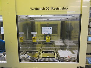
Resist Strip

This resist strip is only for wafers without metal and SU-8.
There are one Remover 1165 bath for stripping and one IPA bath for rinsing.
Here are the main rules for resist strip use:
- Place the wafers in a wafer holder and put them in the first bath for 10 min, this time is depending how much resist you have on the surface.
- After the strip rinse your wafers in the IPA bath for 2-3 min.
- Rinse your wafers for 4-5 min. in running water after stripping.
The user manual and contact information can be found in LabManager: Resist Strip - requires login
Overview of wet bench 06 and 07
| Resist Strip | Lift-off | |
|---|---|---|
| General description | Wet stripping of resist | Lift-off process |
| Chemical solution | NMP Remover 1165 | NMP Remover 1165 |
| Process temperature | Up to 65°C | Up to 65°C |
| Batch size |
1 - 25 wafers |
1 - 25 wafers |
| Size of substrate |
|
|
| Allowed materials |
|
All metals except Type IV (Pb, Te) |
