Specific Process Knowledge/Lithography/EBL
Feedback to this page: click here
Performance of the e-beam writers at DTU Nanolab
| Equipment | JEOL JBX-9500FSZ | Raith Elphy (NOT APPLICABLE) | |
|---|---|---|---|
| Performance | Resolution | ~5 nm beam diameter, ~10 nm lines obtained in 50 nm thick resist (CSAR), 7 nm in HSQ | ~70 nm lines obtained in 50 nm thick resist (CSAR) |
| Maximum writing area without stitching | 1mm x 1mm | 2mm x 2mma | |
| Process parameter range | E-beam voltage | 100 kV | 5-25 kV |
| Scanning speed | 100 MHz | 6 MHz | |
| Min. electron beam size | 4 nm | Not measured | |
| Min. step size | 1 nm | 1 nma | |
| Beam current range | 0.1nA to 60nA in normal conditions | 0.01 to 5 nAa | |
| Dose range | 0.001 - 100000µC/cm2 | 0.000001 µC/cm2 to infinitya,b | |
| Samples | Batch size |
Wafer cassettes:
|
Only chips, max dimension about 20 x 20 mm.
(If at least one dimension is less than 23 mm, bigger chips (e.g. 40 x 20) may be allowed - contact Nanolab) |
| Substrate material allowed |
|
| |
a The Raith tool with the attached LEO SEM allows ample freedom in the choice of most parameters. The limits indicated here refer to best cases and may be further constrained by your current selection of microscope and patterning parameters.
b For all applicable purposes.
E-beam resists
For info regarding E-beam resist in E-beam evaporating equiptment see here: Process information for Wordentec
E-beam resists in the cleanroom
We recommend all groups or users to have their own bottle of e-beam resist inside the cleanroom.
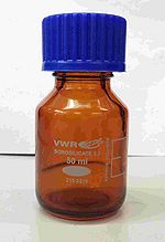
- Find a blue-capped glass bottle in the cupboard next to office 055 in 346 (outside the cleanroom).
- Bring the bottle inside gowning; clean it thoroughly on the outside with water or alcohol
- Bring the bottle to a fumehood inside the cleanroom; clean the bottle and the lid thoroughly on the inside with the main solvent of your resist. For CSAR, ZEP, mr EBL, and most PMMAs, it is anisole. If in doubt which solvent your e-beam resist contains, read the MSDS of the resist to be found here.
- If you need to dilute the resist, find a measurement beaker and clean it thoroughly in same solvent as your own bottle. For CSAR, ZEP, mr EBL, and anisole-based PMMA, you can use the measurement beaker in the box inside the fumehood in E-4.
- Let the bottle dry in the fumehood.
- Bring the (main) bottle of resist to the fumehood. Carefully unscrew the lid of the resist bottle. If necessary, wipe the thread of the resist bottle before you pour resist into your own bottle; dried resists may sit on the thread and be transferred into your bottle (or worse into the large resist bottle) when pouring.
- Clean all bottles on the outside with acetone or IPA, let them fume off in the fumehood. Clean the measurement beaker as well.
- Find a label to your resist bottle; bottles without labels will be removed from the cleanroom.
- Write name, Lotnumber, group and date on your bottle.
When spin coating e-beam resist, you should use a pipette to transfer resist from your bottle to the substrate. If you pour the resist directly from your bottle, you will leave resist in the thread that will soon dry out and leave particles in the resist.
The disposable pipettes need to be thoroughly cleaned with a N2 gun before use (app. 20 s). After some practice, you can obtain particle-free 4" wafers if bottle and pipette (and spin coater) are properly cleaned.
Keep your resist bottles in up-right position, do not tilt or shake them too much, this can spread particles from the sidewall into the resist.
E-beam resists and Process flow
The table describes the e-beam resist used in the cleanroom for standard e-beam exposure. Some of resists are not provided by DTU Nanolab and some are not yet approved for common use in the cleanroom and are currently being tested. If you wish to test some of these resists or other resists, please contact Lithography.
Standard DTU Nanolab resists purchased and tested by DTU Nanolab:
| Resist | Polarity | Manufacturer | Comments | Technical reports | Spin Coater | Thinner | Developer | Rinse | Remover | Process flows (in docx-format) |
| CSAR | Positive | AllResist | Standard positive resist, very similar to ZEP520. | Allresist_CSAR62_English.pdf,, CSAR_62_Abstract_Allresist.pdf | See table here | Anisole | AR-600-546, AR-600-548, N50, MIBK:IPA | IPA | AR-600-71, 1165 Remover | Process Flow CSAR.docx Process Flow CSAR with ESPACER Process Flow CSAR with Al Process Flow LOR5A with CSAR
|
| ZEP520A (not supplied by Nanolab anymore) | Positive resist, contact Lithography if you plan to use this resist | ZEON | Positive resist | ZEP520A.pdf, ZEP520A spin curves on SSE Spinner | See table here | Anisole | ZED-N50/Hexyl Acetate,n-amyl acetate, oxylene. JJAP-51-06FC05.pdf, JVB001037.pdf | IPA | acetone/1165 | Process_Flow_ZEP.docx
|
| Copolymer AR-P 617 | Positive | AllResist | Approved, not tested yet. Used for trilayer (PE-free) resist-stack or double-layer lift-off resist stack. Please contact Lithography for information. | AR_P617.pdf | See table here | PGME | AR 600-55, MIBK:IPA | acetone/1165 | Trilayer stack: Process_Flow_Trilayer_Ebeam_Resist.docx | |
| mr EBL 6000.1 | Negative | MicroResist | Standard negative resist | mrEBL6000 processing Guidelines.pdf | See table here | Anisole | mr DEV | IPA | mr REM | Process_Flow_mrEBL6000.docx
|
| HSQ (XR-1541) | Negative | DOW Corning | Approved. Standard negative resist | HSQ Dow Corning, MSDS HSQ | See table here | TMAH, AZ400K:H2O | H2O | process flow HSQ | ||
| AR-N 8200 | Negative | AllResist | Both e-beam and DUV sensitive resist. Currently being tested, contact Thomas Pedersen for information. | AR 300-47 | H2O | |||||
| AR-N 7520 | Negative | AllResist | Both e-beam, DUV and UV-sensitive resist. Currently being tested, contact Peixiong Shi for information. | AR-N7500-7520.pdf | See table here | PGMEA | AR 300-47, TMAH | H2O |
|
Non-standard DTU Nanolab resists not purchased by DTU Nanolab:
| Resist | Polarity | Manufacturer | Comments | Technical reports | Spinner | Thinner | Developer | Rinse | Remover | Process flows (in docx-format) |
| PMMA | Positive | AllResist | We have various types of PMMA in the cleanroom. Please contact Lithography for information. | See table here | Anisole | MIBK:IPA (1:3), IPA:H2O | IPA | acetone/1165/Pirahna |
| |
| ZEP7000 | Positive | ZEON | Not approved. Low dose to clear, can be used for trilayer (PEC-free) resist-stack. Please contact Lithography for information. | ZEP7000.pdf | See table here | Anisole | ZED-500/Hexyl Acetate,n-amyl acetate, oxylene. | IPA | acetone/1165 | Trilayer stack: Process_Flow_Trilayer_Ebeam_Resist.docx |
| AR-N 7500.18 | Negative | AllResist | Both e-beam, DUV and UV-sensitive resist. Currently being tested, contact Thomas Pedersen for information. | ARN7500.pdf | See table here | PGMEA | MIF726 | H2O |
If the resist is not adhering properly to the substrate, the coating looks like full of pinholes and the edge is not covered, try to remove the resist, dip 30s. in BHF, rinse 5 mins and spin dry, the spin coat again.
Development
There are many different developers for different E-beam resist, but since CSAR and ZEP520A are the most used at Nanolab, we have installed a semi automatic puddle developer: Developer E-beam in E-4.
To accommodate most users, this tool uses developers: AR 600-546 for development of CSAR 6200 resist series and ZED N-50 for ZEP520A resists and IPA as a rinsing step.
Intermediate results indicate that using ZED N-50 for CSAR 6200 series resist will introduce an elevated amount of residues, and vice verva for AR 600 - 546 used on ZEP 520A, but it is inconclusive.
We therefore recommend to use:
- ZED N-50 for Zep520A
- AR 600-546 for CSAR 6200 series
The recipes are divided into different developer and development times.
The recipes 546 are short for AR 600-546 and N-50 is short for ZED N-50.
After the developer there is a time indication eg. 10s, 30s, 60s ect.
Since this system is a spray nozzle that creates a puddle of developer on the substrate the spray is on for 10s. to cover any type of substrates, however this procedure starts the actual development, and the "idle" time is hence shortened accordingly.
The system is setup so that 10s. in the Developer E-beam correlates to 10s. in a beaker, however all designs are different and larger or smaller structures may need different development times.
Cold development
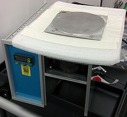
We do have the possibility of making cold development, to get more vertical and smoother sidewalls. We have a coolplate that can go down to -2°C, with a ramp of app. 3 °C/min.
Is it recommended to make a dose test, if one is to transfer from ordinary development to cold.
Procedure
- Pour developer suited for your resist into a small blue cap bottle, and label it, remember to mark it with lot number, date and your name.
- Leave this small bottle of developer in the fridge in Cx1 at least overnight to acclimatize.
- Take the coolplate located in D3 (see picture) and connect it in Fumehood 10 (E-beam) place it on the sink-lid to keep a good airflow.
- Hold left button on the front panel of the cool plate and set temperature with up/down arrows.
- The cool plate can go down to -2°C, and the fridge is +5°C hence use a beaker and pour cold developer into it and place on the coolplate, leave it to acclimatize for the desired temperature.
Development time in cold development, should be subject to testing, depending on structure size and density, but is comparable with "normal" development times.
When developing at low temperatures, condensation can occur
Remember to clean up after you are done
Proximity Error Correction
Even though the electron beam diameter is below 5 nm, the feature and pitch resolution in resist is limited by the forward and backward scattering of the electrons. The forward scattering depends on the electron acceleration voltage, the resist material and thickness. The backward scattering depends on the electron acceleration voltage and the substrate material [1], [2].
As the travel distance of backscattered electrons is fairly large, e-beam patterned structures will be influenced by adjacent e-beam patterned structures, i.e. a proximity effect. These proximity effects can be avoided either by simulating a proximity error correction (PEC) in BEAMER or by using the right stack of e-beam resist.
Proximity Error Correction (PEC) in BEAMER
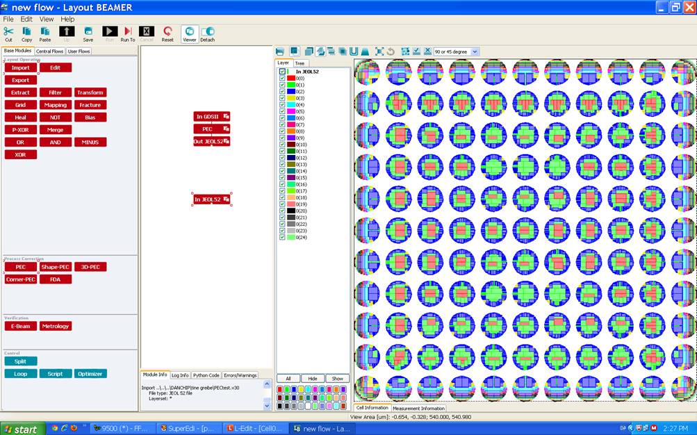
BEAMER is endowed with a software that corrects for proximity errors in the e-beam exposure. You can read more about this function in the BEAMER manual here and in the BEAMER presentation here BEAMERPresentation.pdf.
The proximity error correction require a forward and a backward range parameter, alfa and beta, and a ratio of backscattered energy to the forward scattered energy, eta. As alfa depends on the electron acceleration voltage, which is constant at 100kV, alfa is in BEAMER fixed to 0.007. Help to find beta and eta can be found here.
Alternatively, a point-spread function can be used in BEAMER to calculate the optimised dose-variation.
Trilayer resist stack
As an alternative to PEC, a trilayer reists stack with a thin layer of thermally evaporated Ge can be used [3]. This reists stack has not yet been tested at DTU Nanolab. A process flow for this procedure can be found here Process_Flow_Trilayer_Ebeam_Resist.docx, but please contact Lithography before use.
Charging of non-conductive substrates
All substrates are grounded to the cassette when properly loaded. In a non-conducting substrate, the accumulation of charges in the substrates will however destroy the e-beam patterning. To avoid this, a charge dissipating layer is added on top of the e-beam resist; this will provide a conducting layer for the electrons to escape, while high-energy electrons will pass through the layer to expose the resist.
If you wish to investigate the charge dissipation using other methods than below, please contact Lithography.
ESPACER
Espacer is a chemical that works as a discharging layer; it is spun onto the wafer on top of the resist and easily rinsed off the wafer after e-beam exposure. Visit this page for more information: Espacer
Aluminum coating
At DTU Nanolab, we recommend to use a thin (20 nm) layer of thermally evaporated aluminum on top of the e-beam resist. Preferably, the thickness of Al and the e-beam dose should be optimised to the features you wish to e-beam pattern [4]. A good starting point is 20 nm Al; from here dose and development can be optimised to reach the resolution and feature size required.
The process flow for a standard e-beam exposure on CSAR with Al on top can be found here Process Flow CSAR with Al.
Literature on E-beam Lithography
- Handbook of Microlithography, Micromachining, and Microfabrication, Volume 1: Microlithography, P. Rai-Choudhury (Editor), chapter 2 (p 139 – 250). Link to book can be found here: http://www.cnf.cornell.edu/cnf_spietoc.html
- Lithography, Wiley, 2011: Chapter 3, Electron Beam Lithography by Stefan Landis: http://onlinelibrary.wiley.com/doi/10.1002/9781118557662.ch3/summary


