Specific Process Knowledge/Lithography/Espacer
Espacer is a chemical that works as a discharging layer when e-beam writing on a non-conducting substrate or more than 500nm of dielectric material in on the top surface, this includes resists; it is spun onto the wafer on top of the resist and easily rinsed off the wafer after e-beam exposure.
All substrates are grounded to the e-beam cassette when properly loaded. On a non-conducting substrate, the accumulation of charges in the substrates will however destroy the e-beam patterning. To avoid this, a charge dissipating layer is added on top of the e-beam resist; this will provide a conducting layer for the electrons to escape, while high-energy electrons will pass through the layer to expose the resist.
We have Espacer in stock and approved for use in the cleanroom. You can find a guideline for a process flow here: Process Flow CSAR + ESPACER.docx. Technical information of Espacer can be found here: Espacer_300_Technical_Info.pdf, Espacer_catalog.pdf.
Espacer is a dirty chemical, so we recommend Electra92, or best Thermal Al eg. 20 nm instead
Please contact Lithography if you wish to use this material.
| Process | No ESPACER | ESPACER |
|---|---|---|
| Wafer | Borofloat 4" wafers (JB456), no pretreatment | |
| Resist | AR-P 6200/2 AllResist E-beam resist | |
| Spin Coat | 1 min @ 4000 rpm, softbake 2 min @ 150 degC, thickness ~140nm | |
| ESPACER | 1 min @ 2000 rpm (no softbake), Spin Coater: Manual All Puropse | |
| E-beam exposure | 2 nA, aperture 5, dose 150-310 muC/cm2, SHOT (A,10) | |
| Rinse | Rinsed with hand shower in fumehood, dried with N2 gun | |
| Developing | SX-AR 600-54/6 60 sec, 60 sec IPA rinse | |
| Characterization | Nikon ECLIPSE optical microscope, E-5 | |
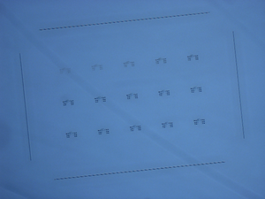
| All doses | 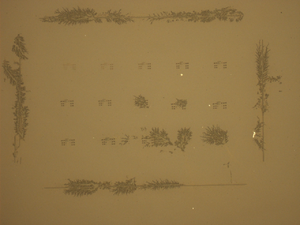
|
|
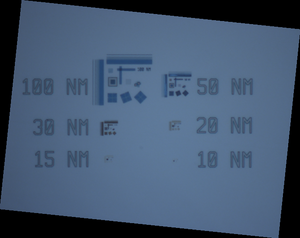
| 230 muC/cm2 | 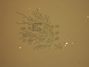
|
|
| 219 muC/cm2 | 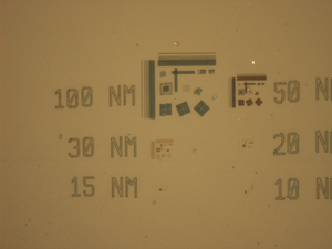
|
|
| Sputter Coated | <10nm Pt at DTU CEN | |
| Characterization | Zeiss SEM supra 60VP, D-2 | |
| 230 muC/cm2 | 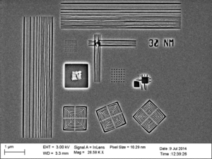
| |