Clean your sample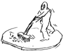
|
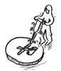
Dry your sample 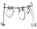
|
Create a thin film on your sample 
|
Dope your sample 
|
Thermal treatment of your sample 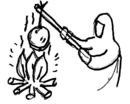
|
Make a mask on your sample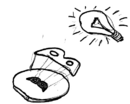
|
Transfer pattern to your sample 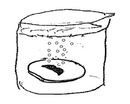
|
Define your structure directly File:Jehandefine.jpg
|
Bond your samples together 
|
Characterize your sample 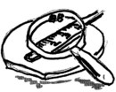
|
Pack your sample 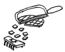
|
|
|
| Clean your sample Clean your sample
|
| Entry page in LabAdviser
|
Techniques
|
Materials
|
| Wafer cleaning
|
Soap Sonic
|
Removes dust and particles
|
| 7-up & Piranha
|
Removes traces of organics and alkali ions
|
| RCA
|
Two step process to remove traces of organics and metals
|
| 5% HF
|
Removes native oxide
|
| IMEC
|
Removing dust, traces of organics and alkali ions and slightly polish the surface.
Make the surface hydrophillic
|
| Dry your sample Dry your sample
|
| Entry page in LabAdviser
|
Techniques
|
Materials
|
| Wafer and sample drying
|
Spin dryers
|
Whole wafers
|
| Critial point dryer
|
Sensitive wafers
|
| Ethanol fume drying
|
Sensitive wafers
|
| N2 blow drying
|
N2 pistols
|
| Create a layer/film on your sample Create a layer/film on your sample
|
| Entry page in LabAdviser
|
Techniques
|
Materials
|
| Thermal Process/Oxidation
|
Thermal oxidation
|
Thermal SiO2
|
| Thin film deposition
|
Sputter deposition
|
Metals: Ti, Cu, Al, Cr, Ag, Au, Pd, Ta, Cu, Ta, W, Mo, Co, Fe, Pt, Mg, Nb, Ni, Ru
Semiconductors: Si, Ge
Oxides: SiO2, ITO, ZnO, Al2O3, Cr2O3, MgO, Ta2O3
Alloys: NiV, MnIr, NiFe, AlCu, CoFe, CuTi, FeMn, NiCo, TiW
|
| Thermal evaporation
|
Al, Ge, Ag
|
| E-beam evaporation
|
Metals: Ti, Cr, Al, Ni, Pt, Au, Mo, Pd, Ag, Cu, W, Ta
Semiconductors: Si, Ge
Oxides: SiO2, TiOs
Alloys: NiCr, TiAl
|
| LPCVD
|
Si3N4, SRN, SiO2, Si (poly and amorph)
|
| PECVD
|
Si3N4, SiO2, PBSG
|
| Electroplating
|
Ni
|
| Epitaxial growth /MOCVD
|
?
|
| Lithography/Coaters
|
Spin coating
|
resists, polymers
|
| Spray coating
|
resists, polymers
|
| Make a mask on your sample Make a mask on your sample
|
| Entry page in LabAdviser
|
Techniques
|
Materials
|
| Lithography
|
Photolithography
|
UV resists
|
| Deep UV lithography
|
DUV resists
|
| E-beam lithography
|
E-beam resists
|
| Imprinting
|
Polymers
|
| Transfer mask pattern to your sample Transfer mask pattern to your sample
|
| Entry page in LabAdviser
|
Techniques
|
Materials
|
| Etch
|
Wet etch
|
Si, Glass, SiO2, Si3N4, Al, Cr, Ti, Au, Pt, InP, InGaAsP, GaAs/AlGaAs
|
| Dry etch
|
Any material
|
| Lithography/Lift-off
|
Lift-off
|
Most materials
|
 Define your structure directly Define your structure directly
|
| Entry page in LabAdviser
|
Techniques
|
Materials
|
| Direct Structure Definition
|
Polymer Injection molding
|
TOPAS
|
| LASER micro machining
|
Silicon, Metal, Graphene (on silicon), Glass (Pyrex, fused silica), TOPAS, PMMA
|
| Dicing saw
|
Silicon, Glass (Pyrex, fused silica)
|
| Imprinting
|
TOPAS, PMMA
|
| Lithography definition
|
SU8, AZ resists
|
| Characterize your sample Characterize your sample
|
| Entry page in LabAdviser
|
What do you need to measure?
|
Technique/Method
|
| Characterization
|
Sample Imaging, XY dimensions
|
Microscopy: optical, SEM, AFM
|
|
|
Sample Topography
|
AFM, Profiling with stylus or optical
|
|
|
Film thickness and optical constants
|
Ellipsometry, Reflectometry, Prism Coupling
|
|
|
Film Stress
|
Profiling with stylus or optical
|
|
|
Wafer thickness
|
Micrometer gauge
|
|
|
Element analysis
|
XPS, EDX, SIMS
|
|
|
Contact Angle
|
|
|
|
Resistivity
|
Four point probe, Probe station
|
|
|
Doping level/Carrier density
|
ECV (Electrochemical Capacitance-Voltage) -profiler
|
|
|
Direct Bandgap
|
Photoluminescence
|
|
|
Lattice mismatch
|
X-ray diffractometer
|
|
|
Defects/contamination
|
Particle/defect counter
|
|
|


.png)