|
|
| Line 375: |
Line 375: |
| | | | | |
| |7-up & Piranha | | |7-up & Piranha |
| |Removes organics and alkali ions | | |Removes traces of organics and alkali ions |
| |- | | |- |
| | | | | |
| |RCA | | |RCA |
| |Two step process to remove organics and metals | | |Two step process to remove traces of organics and metals |
| |- | | |- |
| | | | | |
| Line 387: |
Line 387: |
| | | | | |
| |IMEC | | |IMEC |
| |Removing dust, organics and alkali ions and slightly polish the surface. | | |Removing dust, traces of organics and alkali ions and slightly polish the surface. |
| Make the surface hydrophillic | | Make the surface hydrophillic |
| |- | | |- |
Revision as of 07:11, 17 October 2014
2nd Level - Process Topic
Feedback to this page: click here
Choose the process topic you are interested in
The section below here is under construction 
Overview of sample processing
|
|
Clean your sample
|
Dry your sample 
|
Create a thin film on your sample 
|
Dope your sample 
|
Thermal treatment of your sample 
|
Make a mask on your sample
|
Transfer pattern to your sample 
|
Define your structure directly File:Jehandefine.jpg
|
Bond your samples together 
|
Characterize your sample 
|
Pack your sample 
|
|
|
| Clean your sample Clean your sample
|
| Entry page in LabAdviser
|
Techniques
|
Materials
|
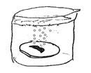
| Wafer cleaning
|
Soap Sonic
|
Removes dust and particles
|
|
|
7-up & Piranha
|
Removes traces of organics and alkali ions
|
|
|
RCA
|
Two step process to remove traces of organics and metals
|
|
|
5% HF
|
Removes native oxide
|
|
|
IMEC
|
Removing dust, traces of organics and alkali ions and slightly polish the surface.
Make the surface hydrophillic
|
| Create a layer/film on your sample Create a layer/film on your sample
|
| Entry page in LabAdviser
|
Techniques
|
Materials
|
| Thermal Process/Oxidation
|
Thermal oxidation
|
Thermal SiO2
|
| Thin film deposition
|
|
|
|
|
Sputter deposition
|
Si,SiO2,Si3N3,TiO2, metals
|
|
|
Thermal evaporation
|
Al, ?
|
|
|
E-beam evaporation
|
Metals
|
|
|
LPCVD
|
Si3N4, SRN, SiO2, Si (poly and amorph)
|
|
|
PECVD
|
Si3N4, SiO2, PBSG
|
|
|
Electroplating
|
Ni
|
|
|
Epitaxial growth /MOCVD
|
?
|
| Lithography/Coaters
|
|
|
|
|
Spin coating
|
resists, polymers
|
|
|
Spray coating
|
resists, polymers
|
| Thermal treatment of your sample Thermal treatment of your sample
|
| Entry page in LabAdviser
|
Techniques
|
Materials
|
| Thermal Process
|
Annealing
|
Si, PECVD layers
|
|
|
Oxidation
|
Si wafers
|
|
|
Doping with B/P
|
Si wafers
|
|
|
Pyrolysis
|
Resists?
|
|
|
Rapid Thermal Anneal (RTP)
|
?
|
| Make a mask on your sample Make a mask on your sample
|
| Entry page in LabAdviser
|
Techniques
|
Materials
|
| Lithography
|
|
|
|
|
Photolithography
|
UV resists
|
|
|
Deep UV lithography
|
DUV resists
|
|
|
E-beam lithography
|
E-beam resists
|
|
|
Imprinting
|
Polymers
|
|
|
Lift-off
|
mostly used for making metal masks
|
| Transfer mask pattern to your sample Transfer mask pattern to your sample
|
| Entry page in LabAdviser
|
Techniques
|
Materials
|
| Etch
|
|
|
|
|
Wet etch
|
Si, Glass, SiO2, Si3N4, Al, Cr, Ti, Au, Pt, InP, InGaAsP, GaAs/AlGaAs
|
|
|
Dry etch
|
Any material
|
| Lithography/Lift-off
|
|
?
|
| Characterize your sample Characterize your sample
|
| Entry page in LabAdviser
|
What do you need to measure?
|
Technique/Method
|
| Characterization
|
Sample Imaging, XY dimensions
|
Microscopy: optical,SEM,AFM
|
|
|
Sample Topography
|
AFM,Profiling with stylus or optical
|
|
|
Film thickness and optical constants
|
Ellipsometry,Reflectometry,Prism Coupling
|
|
|
Film Stress
|
Profiling with stylus or optical
|
|
|
Wafer thickness
|
|
|
|
Element analysis
|
XPS,EDX,SIMS
|
|
|
Contact Angle
|
|
|
|
Resistivity
|
Four point probe
|
|
|
Doping level/Carrier density
|
|
|
|
Photoluminescence
|
|
|
|
jmli test


