|
|
| Line 150: |
Line 150: |
| <br clear="all" /> | | <br clear="all" /> |
|
| |
|
| = Process Pages =
| |
|
| |
| ===[[Specific_Process_Knowledge/Lithography/UVLithography|UV Lithography]]===
| |
| *[[Specific_Process_Knowledge/III-V_Process/photolithography/III_V_Photoresist|Spin Coating of AZ5214E, AZ5206, and LOR7B/AZ5206]]
| |
|
| |
| ===[[Specific Process Knowledge/Lithography/DUVStepperLithography|Deep UV Lithography]]===
| |
| *[[Specific Process Knowledge/Lithography/DUVStepper#Process information|Spin Coater]]
| |
| *[[Specific Process Knowledge/Lithography/DUVStepper#Process information 2|Stepper]]
| |
|
| |
| ===[[Specific Process Knowledge/Lithography/EBeamLithography|E-beam Lithography]]===
| |
| *[[Specific_Process_Knowledge/Lithography/CSAR|Spin curves, dose tests, and etch tests in standard positive resist AR-P 6200 (AllResist)]]
| |
| *[[Specific_Process_Knowledge/Lithography/mrEBL6000| Spin curves and dose tests in mr EBL 6000.1 negative e-beam resist (MircoResist)]]
| |
| *[[Specific_Process_Knowledge/Lithography/ZEP520A|Spin curves of ZEP520A (ZEON)]]
| |
| *[[Specific_Process_Knowledge/Lithography/ARP617|Spin curves of Copolymer AR-P 617.05 (AllResist)]]
| |
| *[[Specific_Process_Knowledge/Lithography/Espacer|Process information on Espacer]]
| |
|
| |
| ===[[Specific Process Knowledge/Lithography/NanoImprintLithography|NanoImprint Lithography]]===
| |
| *[[Specific_Process_Knowledge/Imprinting|Imprinting]]
| |
|
| |
| <br> <br>
| |
|
| |
|
| =Equipment Pages= | | =Equipment Pages= |
Feedback to this page: click here
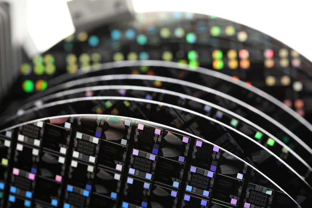
Comparing lithography methods at DTU Danchip
|
|
UV Lithography
|
DUV Stepper Lithography
|
E-beam Lithography
|
Nano Imprint Lithography
|
2-Photon Polymerization Lithography 
|
| Generel description
|
Pattern transfer via UltraViolet (UV) light
|
Pattern transfer via DeepUltraViolet (DUV) light
|
Direct writing via electron beam
|
Pattern transfer via hot embossing(HE)
|
Direct writing via IR laser
|
| Pattern size range
|
|
|
|
|
- 3D voxel through transparent substrate: 0.3 µm diameter; 0.6 µm high
- 2D spot on opaque substrate: 0.6 µm diameter
|
| Resist type
|
- UV sensitive:
- AZ 5214E, AZ 4562, AZ MiR 701 (positive)
- AZ 5214E, AZ nLOF 2020, SU-8 (negative)
|
- DUV sensitive
- JSR KRF M230Y, JSR KRF M35G (positive)
- UVN2300-0.8 (negative)
|
- E-beam sensitive
- ZEP502A, CSAR , PMMA (positive)
- HSQ, Ma-N 2403, AR-N 7520 (negative)
|
|
- UV sensitive:
- IP photoresists, SU-8 (3D)
- AZ resists (2D)
|
| Resist thickness range
|
~0.5µm to 20µm
|
~50nm to 2µm
|
~30nm to 0.5 µm
|
~ 100nm to 2µm
|
droplet or coating
|
| Typical exposure time
|
2s-30s pr. wafer
|
Process depended, depends on pattern, pattern area and dose
|
Depends on dose, Q [µC/cm2], beam current, I [A], and pattern area, A [cm2]: t = Q*A/I
|
Process depended, depends also on heating and cooling temperature rates
|
Process depended, depends on pattern and dose
|
| Substrate size
|
- small samples
- 50 mm wafers
- 100 mm wafers
- 150 mm wafers
|
- 100 mm wafers
- 150 mm wafers
- 200 mm wafers
|
We have cassettes that fit to
- 4 small samples (20mm, 12mm, 8mm, 4mm)
- 6 wafers of 50 mm in size
- 2 wafers of 100 mm in size
- 1 wafer of 150 mm in size
Only one cassette can be loaded at time
|
- small samples
- 50 mm wafers
- 100 mm wafers
- 150 mm wafers
|
- Cover slides
- 50 mm wafers
- 100 mm wafers
- IBIDI
|
| Allowed materials
|
- Any standard cleanroom material
|
- Any standard cleanroom material
|
- Any standard cleanroom material
|
- Any standard cleanroom material
|
- Any standard cleanroom material
|
Equipment Pages
Manuals

