Specific Process Knowledge/Lithography/Coaters: Difference between revisions
| (92 intermediate revisions by 4 users not shown) | |||
| Line 1: | Line 1: | ||
= | {{cc-nanolab}} | ||
'''Feedback to this page''': '''[mailto:labadviser@nanolab.dtu.dk?Subject=Feed%20back%20from%20page%20http://labadviser.nanolab.dtu.dk/index.php?title=Specific_Process_Knowledge/Lithography/Coaters click here]''' | |||
[[Category: Equipment |Lithography coaters]] | [[Category: Equipment|Lithography coaters]] | ||
[[Category: Lithography|Coaters]] | [[Category: Lithography|Coaters]] | ||
__TOC__ | |||
=Coater Comparison Table= | |||
{| border=" | {|border="1" cellspacing="1" cellpadding="10" style="text-align:left;" | ||
!colspan="2" border="none" style="background:silver; color:black;" align="center"|Equipment | !colspan="2" border="none" style="background:silver; color:black;" align="center"|Equipment | ||
|style="background:WhiteSmoke; color:black"|<b>[[Specific_Process_Knowledge/Lithography/Coaters#Spin_Coater:_Gamma_UV|Spin Coater: Gamma UV]]</b> | |style="background:WhiteSmoke; color:black"|<b>[[Specific_Process_Knowledge/Lithography/Coaters#Spin_Coater:_Gamma_UV|Spin Coater: Gamma UV]]</b> | ||
|style="background:WhiteSmoke; color:black"|<b>[[Specific_Process_Knowledge/Lithography/ | |style="background:WhiteSmoke; color:black"|<b>[[Specific_Process_Knowledge/Lithography/DUVStepperLithography#S.C3.9CSS_Spinner-Stepper|Spin Coater: Süss Stepper]]</b> | ||
|style="background:WhiteSmoke; color:black"|<b>[[Specific_Process_Knowledge/Lithography/Coaters#Spin Coater: Gamma E-beam and UV|Spin Coater: Gamma E-beam and UV]]</b> | |style="background:WhiteSmoke; color:black"|<b>[[Specific_Process_Knowledge/Lithography/Coaters#Spin Coater: Gamma E-beam and UV|Spin Coater: Gamma E-beam and UV]]</b> | ||
|style="background:WhiteSmoke; color:black"|<b>[[Specific_Process_Knowledge/Lithography/Coaters#Spin_Coater:_RCD8|Spin Coater: RCD8]]</b> | |style="background:WhiteSmoke; color:black"|<b>[[Specific_Process_Knowledge/Lithography/Coaters#Spin_Coater:_RCD8|Spin Coater: RCD8]]</b> | ||
|style="background:WhiteSmoke; color:black"|<b>[[Specific_Process_Knowledge/Lithography/Coaters# | |style="background:WhiteSmoke; color:black"|<b>[[Specific_Process_Knowledge/Lithography/Coaters#Spin_coater:_Labspin|Spin Coater: LabSpin 02]]</b> | ||
|style="background:WhiteSmoke; color:black"|<b>[[Specific_Process_Knowledge/Lithography/Coaters# | |style="background:WhiteSmoke; color:black"|<b>[[Specific_Process_Knowledge/Lithography/Coaters#Spin_coater:_Labspin|Spin Coater: LabSpin 03]]</b> | ||
|style="background:WhiteSmoke; color:black"|<b>[[Specific_Process_Knowledge/Lithography/Coaters# | |style="background:WhiteSmoke; color:black"|<b>[[Specific_Process_Knowledge/Lithography/Coaters#Spin_Coater:_LabSpin_04|Spin Coater: LabSpin 04]]</b> | ||
|style="background:WhiteSmoke; color:black"|<b>[[Specific_Process_Knowledge/Lithography/Coaters | |style="background:WhiteSmoke; color:black"|<b>[[Specific_Process_Knowledge/Lithography/Coaters#Spray Coater|Spray Coater]]</b> | ||
|- | |- | ||
!style="background:silver; width:100px; color:black;" align="center"|Purpose | !style="background:silver; width:100px; color:black;" align="center"|Purpose | ||
|style="background:LightGrey; color:black"| | |style="background:LightGrey; color:black"| | ||
| Line 27: | Line 32: | ||
**AZ 5214E | **AZ 5214E | ||
|style="background:WhiteSmoke; color:black"| | |style="background:WhiteSmoke; color:black"| | ||
*Coating and baking of | |||
*Coating and baking of | **BARC (DUV42S-6) | ||
** | **KRF M230Y | ||
** | **KRF M35G | ||
* | **UVN2300-0.8 | ||
|style="background:WhiteSmoke; color:black"| | |style="background:WhiteSmoke; color:black"| | ||
*In-line substrate HMDS priming | *In-line substrate HMDS priming | ||
| Line 39: | Line 44: | ||
**AZ MiR 701 (29cps) | **AZ MiR 701 (29cps) | ||
**AZ 4562 | **AZ 4562 | ||
*Edge bead removal on novolac-based resist | *Edge bead removal on novolac-based resist and SU-8 | ||
|style="background:WhiteSmoke; color:black"| | |style="background:WhiteSmoke; color:black"| | ||
*Coating of | *Coating of | ||
| Line 52: | Line 57: | ||
** CSAR, ZEP, PMMA/MMA, HSQ(FOx) | ** CSAR, ZEP, PMMA/MMA, HSQ(FOx) | ||
*Coating of UV resists | *Coating of UV resists | ||
**AZ5214E, AZ4562, AZMiR701, AZnLOF | **AZ5214E, AZ4562, AZMiR701, AZnLOF, SU-8 | ||
*Coating of imprint resists | *Coating of imprint resists | ||
|style="background:WhiteSmoke; color:black"| | |style="background:WhiteSmoke; color:black"| | ||
* Coating of | *Coating of | ||
** | **SU-8 | ||
** | **mr-DWL | ||
* | **other resists | ||
OBS: this tool is in PolyFabLab | |||
|style="background:WhiteSmoke; color:black"| | |style="background:WhiteSmoke; color:black"| | ||
*Spraying imprint resist | *Spraying imprint resist | ||
| Line 65: | Line 70: | ||
*Spraying of other solutions | *Spraying of other solutions | ||
|- | |- | ||
!style="background:silver; color:black" align="center" valign="center" rowspan="3"|Performance | !style="background:silver; color:black" align="center" valign="center" rowspan="3"|Performance | ||
|style="background:LightGrey; color:black"|Substrate handling | |style="background:LightGrey; color:black"|Substrate handling | ||
| Line 73: | Line 79: | ||
|style="background:WhiteSmoke; color:black"| | |style="background:WhiteSmoke; color:black"| | ||
* Cassette-to-cassette | * Cassette-to-cassette | ||
* Vacuum handling | * Vacuum handling and detection | ||
* Vacuum spin chuck | * Vacuum spin chuck | ||
|style="background:WhiteSmoke; color:black"| | |style="background:WhiteSmoke; color:black"| | ||
| Line 89: | Line 95: | ||
|style="background:WhiteSmoke; color:black"| | |style="background:WhiteSmoke; color:black"| | ||
* Single substrate | * Single substrate | ||
* Vacuum | * Vacuum chucks for chips, 4", and 6" | ||
|style="background:WhiteSmoke; color:black"| | |style="background:WhiteSmoke; color:black"| | ||
Can handle almost any sample size and shape | |||
|- | |- | ||
|style="background:LightGrey; color:black"|Permanent media | |style="background:LightGrey; color:black"|Permanent media | ||
|style="background:WhiteSmoke; color:black"| | |style="background:WhiteSmoke; color:black"| | ||
| Line 100: | Line 107: | ||
* PGMEA solvent for backside rinse and spinner bowl cleaning | * PGMEA solvent for backside rinse and spinner bowl cleaning | ||
|style="background:WhiteSmoke; color:black"| | |style="background:WhiteSmoke; color:black"| | ||
* | * DUV42S-6 (BARC) | ||
* | * KRF M230Y resist | ||
* PGMEA for | * KRF M35G resist | ||
* PGMEA solvent for edge bead removal and backside rinse | |||
|style="background:WhiteSmoke; color:black"| | |style="background:WhiteSmoke; color:black"| | ||
* AR-P 6200. | * AR-P 6200.09 (CSAR) for 2", 4", and 6" | ||
* AZ5214E for 2", 4", and 6" | * AZ5214E for 2", 4", and 6" | ||
* AZ MiR 701 (29cps) for 4", and 6" | * AZ MiR 701 (29cps) for 4", and 6" | ||
| Line 111: | Line 118: | ||
* PGMEA solvent for edge bead removal, backside rinse, and spinner bowl cleaning | * PGMEA solvent for edge bead removal, backside rinse, and spinner bowl cleaning | ||
|style="background:WhiteSmoke; color:black"| | |style="background:WhiteSmoke; color:black"| | ||
No permanent media | |||
|colspan="2 | |colspan="2" style="background:WhiteSmoke; color:black"|Only manual dispense | ||
| | |style="background:WhiteSmoke; color:black"|Only manual dispense | ||
|style="background:WhiteSmoke; color:black"| | |style="background:WhiteSmoke; color:black"| | ||
No permanent media | |||
|- | |||
|style="background:LightGrey; color:black"|Manual dispense option | |style="background:LightGrey; color:black"|Manual dispense option | ||
|style="background:WhiteSmoke; color:black"| | |style="background:WhiteSmoke; color:black"| | ||
| Line 124: | Line 131: | ||
|style="background:WhiteSmoke; color:black"| | |style="background:WhiteSmoke; color:black"| | ||
* no manual dispense | * no manual dispense | ||
* syringe dispense (60cc) of PGMEA and anisole-based resist | |||
|style="background:WhiteSmoke; color:black"| | |style="background:WhiteSmoke; color:black"| | ||
* no manual dispense | * no manual dispense | ||
* syringe dispense (30cc) of PGMEA and anisole-based resist | * syringe dispense (30cc) of PGMEA and anisole-based resist (2" only) | ||
|style="background:WhiteSmoke; color:black"| | |style="background:WhiteSmoke; color:black"| | ||
* yes | * yes | ||
* pneumatic dispense for SU-8 resist and EBR solvent | * pneumatic dispense for SU-8 resist and EBR solvent <span style="color:red">OBS: disabled 2024</span> | ||
|colspan="2" style="background:WhiteSmoke; color:black"|Only manual dispense | |||
|style="background:WhiteSmoke; color:black"|Only manual dispense | |||
|style="background:WhiteSmoke; color:black"| | |style="background:WhiteSmoke; color:black"| | ||
Two syringe pumps | |||
|- | |||
!style="background:silver; color:black" align="center" valign="center" rowspan="2"|Process parameter range | !style="background:silver; color:black" align="center" valign="center" rowspan="2"|Process parameter range | ||
|style="background:LightGrey; color:black"|Spindle speed | |style="background:LightGrey; color:black"|Spindle speed | ||
|style="background:WhiteSmoke; color:black"| | |style="background:WhiteSmoke; color:black"| | ||
10 - 6000 rpm | |||
|style="background:WhiteSmoke; color:black"| | |style="background:WhiteSmoke; color:black"| | ||
10 - 6000 rpm | |||
|style="background:WhiteSmoke; color:black"| | |style="background:WhiteSmoke; color:black"| | ||
10 - 6000 rpm | |||
|style="background:WhiteSmoke; color:black"| | |style="background:WhiteSmoke; color:black"| | ||
10 - 5000 rpm (3000 rpm with non-vacuum chuck) | |||
|colspan="2" style="background:WhiteSmoke; color:black"| | |colspan="2" style="background:WhiteSmoke; color:black"| | ||
100 - 8000 rpm (3000 rpm with edge handling chuck) | |||
|style="background:WhiteSmoke; color:black"| | |style="background:WhiteSmoke; color:black"| | ||
100 - 8000 rpm | |||
|style="background:WhiteSmoke; color:black"| | |style="background:WhiteSmoke; color:black"| | ||
|- | |- | ||
|style="background:LightGrey; color:black"|Gyrset | |style="background:LightGrey; color:black"|Gyrset | ||
|style="background:WhiteSmoke; color:black"| | |style="background:WhiteSmoke; color:black"| | ||
no | |||
|style="background:WhiteSmoke; color:black"| | |style="background:WhiteSmoke; color:black"| | ||
no | |||
|style="background:WhiteSmoke; color:black"| | |style="background:WhiteSmoke; color:black"| | ||
no | |||
|style="background:WhiteSmoke; color:black"| | |style="background:WhiteSmoke; color:black"| | ||
optional (max. speed 3000 rpm) | |||
|colspan="2" style="background:WhiteSmoke; color:black"| | |colspan="2" style="background:WhiteSmoke; color:black"| | ||
no | |||
|style="background:WhiteSmoke; color:black"| | |style="background:WhiteSmoke; color:black"| | ||
no | |||
|style="background:WhiteSmoke; color:black"| | |style="background:WhiteSmoke; color:black"| | ||
|- | |- | ||
!style="background:silver; color:black" align="center" valign="center" rowspan="3"|Substrates | !style="background:silver; color:black" align="center" valign="center" rowspan="3"|Substrates | ||
|style="background:LightGrey; color:black"|Substrate size | |style="background:LightGrey; color:black"|Substrate size | ||
| Line 174: | Line 186: | ||
|style="background:WhiteSmoke; color:black"| | |style="background:WhiteSmoke; color:black"| | ||
*100 mm wafers | *100 mm wafers | ||
*150 mm wafers (tool change | *150 mm wafers | ||
*200 mm wafers (may require tool change) | |||
|style="background:WhiteSmoke; color:black"| | |style="background:WhiteSmoke; color:black"| | ||
*2" or 50 mm wafers | *2" or 50 mm wafers | ||
| Line 186: | Line 199: | ||
*100 mm wafers | *100 mm wafers | ||
*150 mm wafer | *150 mm wafer | ||
*small pieces down to | *small pieces down to 5x5 mm2 | ||
|style="background:WhiteSmoke; color:black"| | |style="background:WhiteSmoke; color:black"| | ||
*100 mm wafers | *100 mm wafers | ||
*150 mm wafer | *150 mm wafer | ||
*small pieces down to | *small pieces down to 5x5 mm2 | ||
|style="background:WhiteSmoke; color:black"| | |style="background:WhiteSmoke; color:black"| | ||
Any sample(s) that fit inside machine | |||
|- | |- | ||
|style="background:LightGrey; color:black"|Batch size | |style="background:LightGrey; color:black"|Batch size | ||
|style="background:WhiteSmoke; color:black"| | |style="background:WhiteSmoke; color:black"| | ||
1 - 25 | |||
|style="background:WhiteSmoke; color:black"| | |style="background:WhiteSmoke; color:black"| | ||
1 - 25 | |||
|style="background:WhiteSmoke; color:black"| | |style="background:WhiteSmoke; color:black"| | ||
1 - 25 | |||
|style="background:WhiteSmoke; color:black"| | |style="background:WhiteSmoke; color:black"| | ||
1 | |||
|colspan="2" style="background:WhiteSmoke; color:black"| | |colspan="2" style="background:WhiteSmoke; color:black"| | ||
1 | |||
|style="background:WhiteSmoke; color:black"| | |style="background:WhiteSmoke; color:black"| | ||
1 | |||
|style="background:WhiteSmoke; color:black"| | |style="background:WhiteSmoke; color:black"| | ||
1 | |||
|- | |- | ||
| style="background:LightGrey; color:black"|Allowed materials | | style="background:LightGrey; color:black"|Allowed materials | ||
|style="background:WhiteSmoke; color:black"| | |style="background:WhiteSmoke; color:black"| | ||
*Silicon | *Silicon | ||
*Glass | *Glass | ||
'''No resist or crystalbond allowed in the HMDS module''' | |||
|style="background:WhiteSmoke; color:black"| | |style="background:WhiteSmoke; color:black"| | ||
*Silicon | *Silicon | ||
| Line 222: | Line 238: | ||
*III-V materials | *III-V materials | ||
*Glass | *Glass | ||
'''No resist or crystalbond allowed in the HMDS module''' | |||
|style="background:WhiteSmoke; color:black"| | |style="background:WhiteSmoke; color:black"| | ||
All cleanroom materials except III-V materials | |||
|colspan="2" style="background:WhiteSmoke; color:black"| | |colspan="2" style="background:WhiteSmoke; color:black"| | ||
*Silicon | *Silicon | ||
| Line 229: | Line 247: | ||
*Glass | *Glass | ||
|style="background:WhiteSmoke; color:black"| | |style="background:WhiteSmoke; color:black"| | ||
All PolyFabLab materials | |||
|style="background:WhiteSmoke; color:black"| | |style="background:WhiteSmoke; color:black"| | ||
*All chemicals to be spray coated must be approved specifically for spray coating | *All chemicals to be spray coated must be approved specifically for spray coating | ||
| Line 239: | Line 257: | ||
=Spin coating= | =Spin coating= | ||
The | The typical spin coating process consists of the following steps: | ||
#Priming (typically HMDS) followed by cooling to room temperature | |||
#Resist dispense (rotation: static or dynamic rotation)(arm: stationary or moving) | |||
#*Optional: Acceleration to a low spin speed if dynamic dispense is used | |||
#*Optional: Resist spreading at low spin speed for spreading thicker resists | |||
#Spin-off | |||
#Backside rinse (typically during spin-off) | |||
#Optional: Edge-bead removal | |||
#Softbake (contact or proximity) | |||
#Cooling to room temperature | |||
* | |||
After priming, the wafer is cooled to room temperature and then transferred to the spin coater. If static dispense is used, the wafer is not rotating during the resist dispense. In the case of dynamic dispense, the wafer rotates at low spin speed during the dispense. The dispense arm is normally stationary during dispense, but some substrates may require the arm to move slowly across the substrate area while dispensing. Moving arm dispensing is usually only done with a rotating substrate. | |||
Using too high spin speed during dispense can cause surface wetting issues, while a too low spin speed causes the resist to flow onto the backside of the wafer. After dispense, a short spin at low spin speed may be used in order to spread the resist over the wafer surface before spin-off. | |||
Spin | ==Spin-off== | ||
The spin-off cycle determines the thickness of the resist coating. For a given resist, the thickness is primarily a function of the spin-off speed and the spin-off time, both following an inverse power-law: | |||
< | <math>y = k \sdot x^{-a}</math> | ||
The acceleration to the spin-off speed also influences the thickness, but the effect is dependent on previous steps. The spin-off is usually a simple spin at one speed, but it may be comprised of several steps at different spin speeds. After spin-off, the wafer is decelerated. | |||
The coated thickness, <math>t</math>, as a function of the spin-off speed, <math>w</math>, follows an inverse power-law: | |||
= | <math>t=k \sdot w^{-a}</math> | ||
The constant, <math>k</math>, is a function of the resist viscosity and solid content, as well as the spin-off time. The exponent, <math>a</math>, is dependent on solvent evaporation, and is typically ~½ for UV resists. This means that from the thickness <math>t_1</math> achieved at spin speed <math>w_1</math>, one can estimate the spin speed <math>w_2</math> needed to achieve thickness <math>t_2</math> using the relation: | |||
<math>t_1 \sdot w_1^{1/2} = t_2 \sdot w_2^{1/2} \rArr w_2 = w_1 \sdot \frac{t_1^2}{t_2^2}</math> | |||
For thick SU-8, however, <math>a</math> is observed to be ~1 (probably due to the low solvent content and/or the formation of skin). In this case, the relation simply becomes: | |||
<math>t_1 \sdot w_1 = t_2 \sdot w_2 \rArr w_2 = w_1 \sdot \frac{t_1}{t_2}</math> | |||
==Backside rinse== | |||
If the spin speed is too low during resist dispense, resist may creep over the edge of the wafer and onto the backside. Some resist tend to leave fine strings of resist protruding from the edge of the wafer, or folded onto the backside, an effect sometimes referred to as "cotton candy". | |||
Any resist on the edge and backside of the wafer will contaminate the end effector, softbake hotplate, and subsequent wafers. | |||
In a backside rinse step, solvent administered through a nozzle to the backside of the wafer, while spinning at low or medium spin speed, dissolves the resist and washes it away. After the rinse, a short spin at medium spin speed dries the wafer before the softbake. | |||
During the backside rinse solvent inevitably creeps onto the front side of the wafer. This effect may be used to dissolve and subsequently remove an edge-bead, but it may also leave the rim of the wafer exposed. As an alternative to backside rinse, a wafer, which is contaminated on the backside, may be softbaked in proximity, in order to protect the hotplate from contamination. This leaves front side coating intact, but also leaves the backside dirty. | |||
==Edge bead== | |||
During spin coating, resist builds up at the edge of the wafer due to the change in surface tension at the edge, as well as extra drying from turbulence created by the wafer edge. | |||
This phenomenon is called edge-bead. Dependent on spin coating parameters, the coating may be several times thicker at the edge than in the central area. In a subsequent hard contact exposure step (mask aligner), this edge-bead introduces an undesired proximity gap, which reduces the lateral resolution, and may even cause the wafer to stick to the mask. | |||
In an edge-bead removal step, solvent administered through a nozzle positioned at the edge of the wafer, while spinning at low or medium spin speed, dissolves the resist and washes it away. After the removal, a short spin at medium spin speed dries the wafer before the softbake. Dependent on the viscosity (solvent content) of the resist after the edge-bead removal, this drying spin may cause the resist to re-flow and create a secondary edge-bead. In some cases, it may be necessary to (partially) softbake the resist before edge-bead removal. | |||
==Softbake== | |||
After spin coating, the solvent in the resist must be evaporated in a baking step, in order to solidify the resist. This softbake can be carried out as a contact bake or a proximity bake. In a contact bake, the wafer is held in close contact to the hotplate surface, either in direct contact on the manual hotlpates or by resting on shallow bumps 150 µm above the hotplate in the Gamma tools. In a proximity bake, the wafer is first moved into proximity, e.g. 1mm, of the hotplate surface, then held there (on the lift pins) for the duration of the bake. | |||
=Spin coaters at DTU Nanolab= | |||
{{:Specific Process Knowledge/Lithography/Coaters/GammaUV}} | |||
{{:Specific Process Knowledge/Lithography/Coaters/GammaDUV}} | |||
{{:Specific Process Knowledge/Lithography/Coaters/GammaEbeam}} | |||
{{:Specific Process Knowledge/Lithography/Coaters/RCD8}} | |||
{{:Specific Process Knowledge/Lithography/Coaters/labspin}} | |||
{{:Specific Process Knowledge/Lithography/Coaters/labspin04}} | |||
{{:Specific Process Knowledge/Lithography/Coaters/sprayCoater}} | |||
=== | =Decommisioned tools= | ||
<span style="color:red">The spin track was decommissioned 2018-02-01.</span> | |||
[[Specific Process Knowledge/Lithography/Coaters/Spin_Track_1_%2B_2_processing|Information about decommissioned tool can be found here.]] | |||
Latest revision as of 13:32, 13 January 2026
The content on this page, including all images and pictures, was created by DTU Nanolab staff, unless otherwise stated.
Feedback to this page: click here
Coater Comparison Table
| Equipment | Spin Coater: Gamma UV | Spin Coater: Süss Stepper | Spin Coater: Gamma E-beam and UV | Spin Coater: RCD8 | Spin Coater: LabSpin 02 | Spin Coater: LabSpin 03 | Spin Coater: LabSpin 04 | Spray Coater | |
|---|---|---|---|---|---|---|---|---|---|
| Purpose |
|
|
|
|
|
OBS: this tool is in PolyFabLab |
| ||
| Performance | Substrate handling |
|
|
|
|
|
|
Can handle almost any sample size and shape | |
| Permanent media |
|
|
|
No permanent media |
Only manual dispense | Only manual dispense |
No permanent media | ||
| Manual dispense option |
|
|
|
|
Only manual dispense | Only manual dispense |
Two syringe pumps | ||
| Process parameter range | Spindle speed |
10 - 6000 rpm |
10 - 6000 rpm |
10 - 6000 rpm |
10 - 5000 rpm (3000 rpm with non-vacuum chuck) |
100 - 8000 rpm (3000 rpm with edge handling chuck) |
100 - 8000 rpm |
||
| Gyrset |
no |
no |
no |
optional (max. speed 3000 rpm) |
no |
no |
|||
| Substrates | Substrate size |
|
|
|
|
|
|
Any sample(s) that fit inside machine | |
| Batch size |
1 - 25 |
1 - 25 |
1 - 25 |
1 |
1 |
1 |
1 | ||
| Allowed materials |
No resist or crystalbond allowed in the HMDS module |
|
No resist or crystalbond allowed in the HMDS module |
All cleanroom materials except III-V materials |
|
All PolyFabLab materials |
| ||
Spin coating
The typical spin coating process consists of the following steps:
- Priming (typically HMDS) followed by cooling to room temperature
- Resist dispense (rotation: static or dynamic rotation)(arm: stationary or moving)
- Optional: Acceleration to a low spin speed if dynamic dispense is used
- Optional: Resist spreading at low spin speed for spreading thicker resists
- Spin-off
- Backside rinse (typically during spin-off)
- Optional: Edge-bead removal
- Softbake (contact or proximity)
- Cooling to room temperature
After priming, the wafer is cooled to room temperature and then transferred to the spin coater. If static dispense is used, the wafer is not rotating during the resist dispense. In the case of dynamic dispense, the wafer rotates at low spin speed during the dispense. The dispense arm is normally stationary during dispense, but some substrates may require the arm to move slowly across the substrate area while dispensing. Moving arm dispensing is usually only done with a rotating substrate.
Using too high spin speed during dispense can cause surface wetting issues, while a too low spin speed causes the resist to flow onto the backside of the wafer. After dispense, a short spin at low spin speed may be used in order to spread the resist over the wafer surface before spin-off.
Spin-off
The spin-off cycle determines the thickness of the resist coating. For a given resist, the thickness is primarily a function of the spin-off speed and the spin-off time, both following an inverse power-law:
The acceleration to the spin-off speed also influences the thickness, but the effect is dependent on previous steps. The spin-off is usually a simple spin at one speed, but it may be comprised of several steps at different spin speeds. After spin-off, the wafer is decelerated.
The coated thickness, , as a function of the spin-off speed, , follows an inverse power-law:
The constant, , is a function of the resist viscosity and solid content, as well as the spin-off time. The exponent, , is dependent on solvent evaporation, and is typically ~½ for UV resists. This means that from the thickness achieved at spin speed , one can estimate the spin speed needed to achieve thickness using the relation:
For thick SU-8, however, is observed to be ~1 (probably due to the low solvent content and/or the formation of skin). In this case, the relation simply becomes:
Backside rinse
If the spin speed is too low during resist dispense, resist may creep over the edge of the wafer and onto the backside. Some resist tend to leave fine strings of resist protruding from the edge of the wafer, or folded onto the backside, an effect sometimes referred to as "cotton candy".
Any resist on the edge and backside of the wafer will contaminate the end effector, softbake hotplate, and subsequent wafers.
In a backside rinse step, solvent administered through a nozzle to the backside of the wafer, while spinning at low or medium spin speed, dissolves the resist and washes it away. After the rinse, a short spin at medium spin speed dries the wafer before the softbake.
During the backside rinse solvent inevitably creeps onto the front side of the wafer. This effect may be used to dissolve and subsequently remove an edge-bead, but it may also leave the rim of the wafer exposed. As an alternative to backside rinse, a wafer, which is contaminated on the backside, may be softbaked in proximity, in order to protect the hotplate from contamination. This leaves front side coating intact, but also leaves the backside dirty.
Edge bead
During spin coating, resist builds up at the edge of the wafer due to the change in surface tension at the edge, as well as extra drying from turbulence created by the wafer edge.
This phenomenon is called edge-bead. Dependent on spin coating parameters, the coating may be several times thicker at the edge than in the central area. In a subsequent hard contact exposure step (mask aligner), this edge-bead introduces an undesired proximity gap, which reduces the lateral resolution, and may even cause the wafer to stick to the mask.
In an edge-bead removal step, solvent administered through a nozzle positioned at the edge of the wafer, while spinning at low or medium spin speed, dissolves the resist and washes it away. After the removal, a short spin at medium spin speed dries the wafer before the softbake. Dependent on the viscosity (solvent content) of the resist after the edge-bead removal, this drying spin may cause the resist to re-flow and create a secondary edge-bead. In some cases, it may be necessary to (partially) softbake the resist before edge-bead removal.
Softbake
After spin coating, the solvent in the resist must be evaporated in a baking step, in order to solidify the resist. This softbake can be carried out as a contact bake or a proximity bake. In a contact bake, the wafer is held in close contact to the hotplate surface, either in direct contact on the manual hotlpates or by resting on shallow bumps 150 µm above the hotplate in the Gamma tools. In a proximity bake, the wafer is first moved into proximity, e.g. 1mm, of the hotplate surface, then held there (on the lift pins) for the duration of the bake.
Spin coaters at DTU Nanolab
Spin Coater: Gamma UV
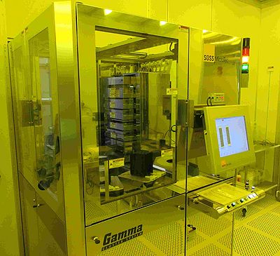
Spin Coater: Gamma UV was installed at DTU Nanolab in March 2015. It is a Gamma 2M cluster from Süss MicroTec with spin coating, HMDS vapour priming, and baking modules.
The system handles 4" and 6" wafers without size conversion, and can be set up to handle 2" or 8".
The coater is equipped with 3 different resist lines, as well as 1 syringe line:
- AZ MiR 701
- AZ nLOF 2020
- AZ 5214E
- Syringe, which can be used for various resists
The processes that are available on the system are developed by Nanolab. Upon request, it is possible to establish new processes. Use of the syringe requires special training, and would as a starting point require batches in excess of 20 wafers.
Link to information about coater chuck size and hotplate pin positions.
The user manual, quality control procedures and results, user APVs, and contact information can be found in LabManager - requires login
Process information
| Purpose |
| |
|---|---|---|
| Resist |
| |
| Performance | HMDS contact angle |
60 - 80° |
| Coating thickness |
| |
| Process parameters | Priming temperature |
120 °C |
| Spin speed |
10 - 6000 rpm | |
| Spin acceleration |
10 - 10000 rpm/s | |
| Hotplate temperature |
25 - 200 °C | |
| Cool plate temperature |
21 °C | |
| Substrates | Substrate size |
|
| Allowed materials |
Silicon and glass Resists and crystalbond are not allowed in the HMDS module | |
| Batch |
1 - 25 |
1) Requires tool change.
Spin coater: Süss stepper
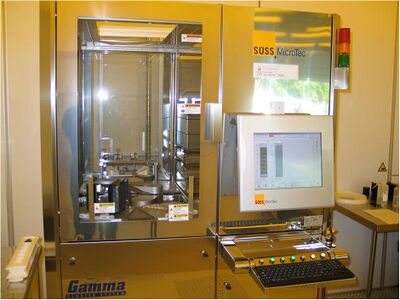
This spinner is dedicated for spinning DUV resists. The spinner is fully automatic and can run up to 25 substrates in a batch 4", 6", and 8" size (8" requires tool change). The machine is equipped with the 3 resist lines (DUV42S-6, KRF M230Y, and KRF M35G), as well as a syringe dispense system.
The user manual, quality control procedures and results, user APVs, and contact information can be found in LabManager:
Equipment info in LabManager - requires login
DUV resist overview
The spinning process will be performed by the customer together with the Photolith group of Nanolab. In case you would like to do DUV lithography, please contact Lithography team, who will consult you and run your wafers together with you.
Bottom Anti Reflection Coating (BARC):
Positive DUV resist for spin coating in 600-300nm thickness range:
Positive DUV resist for spin coating in 1600-800nm thickness range:
Negative DUV resist for spin coating in 1400-800nm or diluted with EC Solvent in 1:1 in 400-200nm thickness range:
- Manufacturers website: UVN2300-0.8
- Datasheet: UVN2300-0.8 - requires login
Process information
| Purpose |
| ||
|---|---|---|---|
| Resist |
| ||
| Performance | Coating thickness |
| |
| Process parameters | Spin speed |
10 - 5000 rpm | |
| Spin acceleration |
100 - 10000 rpm/s | ||
| Hotplate temperature |
| ||
| Substrates | Substrate size |
| |
| Allowed materials |
| ||
| Batch |
1 - 25 | ||
Spin Coater: Gamma E-beam and UV
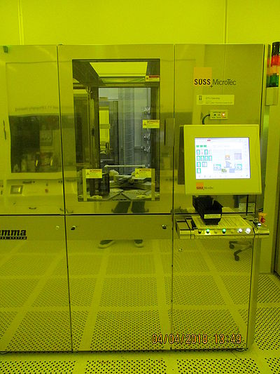
Spin Coater: Gamma E-beam and UV was installed at DTU Nanolab in June 2017. It is a Gamma 4M cluster from Süss MicroTec with spin coating, HMDS vapour priming, and baking modules. The system handles 2", 4", and 6" wafers without size conversion, using two separate coater stations.
The 2" coater station is equipped with 1 resist line, as well as 1 syringe line:
- AR-P 6200.09 (CSAR)
- Syringe, which can be used for various resists (anisole-based or PGMEA-based). We currently recommend against using the syringe, as the process setup is quite demanding. Use a manual spin coater instead.
The 4"/6" coater station is equipped with 4 different resists lines:
- AZ 5214E
- AZ MiR 701
- AR-P 6200.09 (CSAR)
- AZ 4562
The processes that are available on the system are developed by Nanolab. Upon request, it is possible to establish new processes. Use of the syringe requires special training, and requires batch processing - it is not for processing a few wafers now and then.
Link to information about coater chuck size and hotplate pin positions.
The user manual, quality control procedures and results, user APVs, and contact information can be found in LabManager - requires login
Process information
| Purpose |
| |
|---|---|---|
| Resist |
| |
| Performance | HMDS contact angle |
60 - 80° (on Silicon) |
| Coating thickness |
| |
| Process parameters | Priming temperature |
120 °C |
| Spin speed |
10 - 6000 rpm | |
| Spin acceleration |
10 - 10000 rpm/s | |
| Hotplate temperature |
25 - 200 °C | |
| Cool plate temperature |
21 °C | |
| Substrates | Substrate size |
|
| Allowed materials |
Silicon, III-V, and glass Resists and crystalbond are not allowed in the HMDS module | |
| Batch |
1 - 25 |
Spin Coater: RCD8
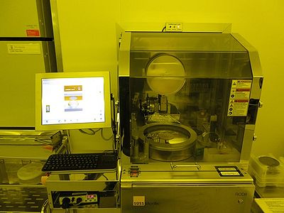
Spin Coater: RCD8 is a model RCD8 T spin coater from Süss MicroTec with a motorized media arm and Gyrset functionality. It's primary purpose is spin coating of SU-8 resist. The media arm was disabled in 2024.
However, due to the possibility of using a non-vacuum chuck, the spin coater is also suitable for coating of substrates with e.g. textured backsides or membranes.
The user manual, user APV, and contact information can be found in LabManager - requires login
Process information
| Purpose |
| |
|---|---|---|
| Resist |
| |
| Performance | Coating thickness |
|
| Process parameters | Spin speed |
Vacuum chuck: 10 - 5000 rpm |
| Spin acceleration |
10 - 3000 rpm/s | |
| Substrates | Substrate size |
|
| Allowed materials |
All cleanroom materials ? | |
| Batch |
1 |
Spin coater: Labspin
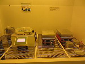
|
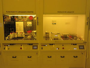
|
| Spin Coater: Labspin 02 | Spin Coater: Labspin 03 + fumehood 11 |
| Loacted in wetbench 08 in E-5 | Located in wetbench 09 in E-5 |
| LabSpin 6, Süss MicroTec | LabSpin 6, Süss MicroTec |
Training video: LabSpin02 + 03
Process information
Spin curves (LabSpin 6):
More information on resists (incl. spin curves) is available in the resist overview.
Available bowlsets:
| Bowlset name | Component solvent | Cleaning solvent | List of resists | Comments |
|---|---|---|---|---|
| AZ resist | PGMEA/Ethyl Lactate | Acetone |
AZ 5214E |
Two bowlsets available |
| CSAR/ZEP/mrEBL/PMMA | Anisole | Remover 1165 |
AR-P 6200 series (CSAR 62) |
|
| HSQ/AR-N 8200 | MIBK/PGME/n-Butyl acetate | Acetone |
HSQ (FOx series) |
|
| OrmoComp/OrmoStamp | Propyl Acetate | Acetone |
OrmoComp |
|
| BCB/CYCLOTENE | Mesitylene | T1100 |
3022-X |
|
| Epoxy/Acrylate | Cyclopentanone/PGMEA/PGME/GBL | Acetone |
SU-8 3000 series |
|
| AR-P 617/AR-N 7520 New | PGME/PGMEA | Acetone | AR-N 7500 series | |
| Polymer Ps-b-PDMS/block copolymer | Heptane | Ethyl Acetate | ||
| DIRTY bowlset | Anything Organic | Use the appropriate cleaning reagent for your resist |
| Purpose | Labspin |
Spin coating of resist ONLY in dedicated bowlsets Please do NOT use substances which is not for the dedicated bowlsets |
|---|---|---|
| Dirty bowlset |
Spin coating of other substances in dirty bowlset
| |
| Process parameters | Spin speed |
|
| Spin acceleration |
| |
| Substrates | Substrate size |
|
| Allowed materials |
All cleanroom materials Please ONLY use substances which is for the dedicated bowlsets in labspins | |
| Batch |
1 |
Spin Coater: LabSpin 04

Spin Coater: LabSpin 04 is a model LabSpin6 TT spin coater from SUSS. It's primary purpose is spin coating of SU-8 resist. It was installed in PolyFabLab in 2025.
The user manual, user APV, and contact information can be found in LabManager - requires login
Training video (same tool in Cleanroom 346): LabSpin02 + 03
Process information
Useful information about resist dispense can be found here.
| Purpose |
| |
|---|---|---|
| Resist |
| |
| Performance | Coating thickness |
Coating thickness range is dependent on specific resist formulation |
| Process parameters | Spin speed |
100 - 8000 rpm |
| Spin acceleration |
200 - 4000 rpm/s (wrongly labelled 1/s^2 in the software) | |
| Substrates | Substrate size |
|
| Allowed materials |
All PolyFabLab materials | |
| Batch |
1 |
Spray Coater
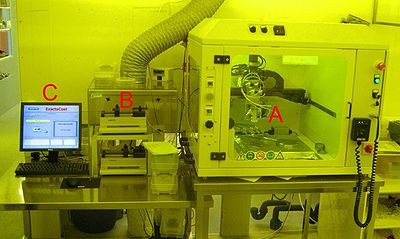
The spray coater at DTU Nanolab is located in Cleanroom C-1. The machine is an ExactaCoat from Sono-tek which can be fitted with one of three different nozzles depending on the nature of the spray coating tasks at hand. The three different nozzles (Impact, AccuMist and Vortex) are optimized for different applications such as spray coating of large areas (e.g. entire wafers), smaller areas (e.g. wafer pieces or other small samples) or already structured samples that cannot be coated uniformly by spin coating. All nozzles use an ultrasonic tranducer for atomizing the solution to be spray coated. It is therefore a prerequisite that all components are compatible with this process. This is the case with most substances, although process parameters may need optimization to give satisfactory results.
Practically any sample that will fit inside the spray coater can be processed. Spray patterns are easily programmed either using predefined spray patterns (1D line, 2D rectangles/circles/meanders/spirals) or custom 3D spray patterns.
The spray coating process as well as major features of the three nozzles are described into more detail in the manual which can be found via the Equipment Info page in LabManager under the Documents sections. The manual can also be found in Labmanager - requires login
Further information about the spray coater (manual, process log, technical information etc.) can be found in LabManger:
Spray coater in LabManager - requires login
Process development
Spray coating using TI spray:
The TI spray resist is the standard spray coater resist used at DTU Nanolab. It requires no dilution and performs well.
Spray coating using other resists:
Other resists are allowed, but most require dilution, as the spray coater will not work with any resist viscosity higher than 20 cP.
| Equipment | Spray Coater | |
|---|---|---|
| Purpose |
| |
| Performance | Substrate handling |
|
| Permanent media |
| |
| Manual dispense option |
| |
| Process parameter range | Solution viscosity |
|
| Chemical properties |
| |
| Substrates | Batch size |
|
| Allowed materials |
| |
Decommisioned tools
The spin track was decommissioned 2018-02-01.
