Specific Process Knowledge/Lithography/Coaters/Spin Coater: Gamma E-beam and UV processing
This section, including all images and pictures, is created by DTU Nanolab staff unless otherwise stated.
Feedback to this page: click here
General Process Information
Processing using Spin Coater: Gamma E-beam and UV is divided into four parts:
- HMDS priming
- Spin coating
- Soft baking
- Edge bead removal
Features of Spin Coater: Gamma E-beam and UV
- Cassette-to-cassette wafer handling
- In-line HMDS priming
- Edge bead removal
- Coater1 for 2" processing
- Coater2 for 4" and 6" processing
HMDS priming
The process of HMDS priming on Spin Coater: Gamma E-beam and UV consists of five steps:
- Dehydration
- HMDS injection
- Reaction
- Purging
- Cooling
The top and bottom heaters of the VPO module are set to 120°C. The wafer is baked under a low vacuum (~0.2 bar) in order to heat and dehydrate the wafer before HMDS application. The HMDS is injected into the process chamber using nitrogen as a carrier gas. 5 liters per minute of dry nitrogen is bubbled through liquid HMDS before flowing into the chamber. The injection lasts until a trip point pressure (~0.7 bar) is reached in the chamber. After the reaction time, the chamber is pumped out, then purged using nitrogen. Finally, the wafer is cooled on the cool plate.
The contact angle after HMDS priming is a function of the priming temperature, the priming time, and the surface condition of the wafer. The condition of the substrate surface is again a function of the substrate type, the substrate history, and the effectiveness of the dehydration step. Since the vapor pressure of water at the chamber temperature is much higher than the dehydration pressure, similarly the boiling point of water at the dehydration pressure is well below the chamber temperature, the dehydration can probably be considered to be quite effective. However, for thick oxides, transport effects may cause the 30s dehydration time to be insufficient to dehydrate the surface sufficiently.
Spin coating
The process of spin coating on Spin Coater: Gamma E-beam and UV consists of a selection of the following steps:
- Acceleration to a low spin speed if dynamic dispense is used
- Resist dispense
- Spin-off
- Backside rinse using PGMEA
The wafer is first centered on the spindle chuck and held in place by vacuum. If static dispense is specified in the process, the spindle remains static during the ensuing resist dispense. In the case of dynamic dispense, the spindle is accelerated to a low spin speed before the resist is dispensed. Using too high spin speed during dispense can cause surface wetting issues, while a too low spin speed causes the resist to flow onto the backside of the wafer. The resist is dispensed through the dispense arm, positioned over the center of the wafer. The resist pump administers a volume of resist which depends on the substrate size.
The spin-off cycle determines the thickness of the resist coating. The thickness is primarily a function of the spin-off speed and the spin-off time, both following an inverse power-law.. The acceleration to the spin-off speed also influences the thickness, but the effect is dependent on previous steps. The spin-off is usually a simple spin at one speed, but it may be comprised of several steps at different spin speeds. After spin-off, the wafer is decelerated.
Dependent on the spin speeds used in the various steps of the spin coating, resist may creep over the edge of the wafer and onto the backside. Also, some resists tend to leave fine strings of resist protruding from the edge of the wafer, or folded onto the backside, an effect sometimes referred to as "cotton candy". This resist will contaminate the soft bake hotplate, and thus subsequent wafers with resist. In a backside rinse step, solvent administered through a nozzle to the backside of the wafer while spinning dissolves the resist and washes it away. After the rinse, a short spin dries the wafer before the soft bake. Backside rinse may be done as part of the spin-off step(s). During the backside rinse solvent inevitably creeps onto the front side of the wafer, and may remove the resist coating on the edge of the wafer. As an alternative to backside rinse, a wafer which is left dirty on the backside by the spin coat process may be soft baked in proximity in order to protect the hotplate from contamination. This leaves front side coating intact, but also leaves the backside dirty.
Soft baking
After spin coating, the solvent in the resist formulation must be evaporated in a baking step in order to solidify the resist. This soft bake can be carried out as a contact bake or a proximity bake. In a contact bake, the wafer is held in close contact to the hotplate surface while resting on shallow bumps only 150µm above the hotplate. In a proximity bake, the wafer is first moved into proximity, e.g. 1mm, of the hotplate surface, then held there (on the lift pins) for the duration of the bake. The hotplate temperatures of the baking modules of Spin Coater: Gamma E-beam and UV are set at temperatures relevant to the resist used, typically 90-110°C for UV resists and 150-200°C for E-beam resists. After baking, the wafer is cooled for 20-60 seconds on the cool plate, depending on the soft bake temperature.
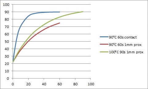
The graphs show temperature profiles of different soft bake recipes. The 90°C 60s contact recipe reaches 90°C after approximately 40s, while the 90°C 60s 1mm prox recipe only reaches 75°C at the end of the soft bake. The 100°C 90s 1mm prox recipe reaches 83°C after 60s and 90°C at the end of the soft bake.
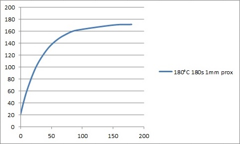
The 180°C 180s 1mm prox recipe reaches 160°C in 90s and finishes at 172°C.
- Temperature profiles of different soft bake recipes in Spin Coater: Gamma e-beam & UV
UV resist soft bake recipes
E-beam resist soft bake recipe


Cooling
After priming and soft bake, the wafers are cooled on the cool plate in order to reduce the temperature before spin coating or delivery to the output cassette. This cooling can be carried out quickly or slowly. In the quick cooling, the wafer is held in close contact to the cool plate surface while resting on shallow bumps only 150µm above the hotplate for 20s. In the slow cooling, the wafer is first moved into 1mm proximity of the cool plate surface and held there (on the lift pins) for 30s, then moved into contact for 20s.
The graphs show temperature profiles of quick and slow cooling from different temperatures. Quick cooling from 90°C initially cools at 8°C/s and reaches 27°C at the end of the recipe. Slow cooling cools at a much lower 2°C/s, and reaches 23°C at the end of the recipe. For comparison, the temperature profiles of 1 minute on the robot arm (presumably the same as on the storage slot or in the output cassette) and 1 minute inside the hotplate (i.e. on top of the lift pins in unload position, 12mm proximity) are shown.
Quick cooling from 120°C initially cools at 11°C/s and reaches 29°C at the end of the recipe. This is thus the temperature at which the wafer is put on the spin coater after HMDS priming. If slow cooling is used, the cooling rate drops to 3°C/s and the wafer reaches 24°C at the end of the recipe.
Quick cooling from 180°C initially cools at 18°C/s and reaches only 34°C at the end of the recipe. Slow cooling cools at a much more reasonable 5°C/s, and reaches 26°C at the end of the recipe.
- Temperature profiles of different cooling recipes in Spin Coater: Gamma e-beam & UV
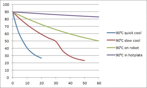
Quick and slow cooling from 90°C, along with cooling on the robot and cooling inside the hotplate module
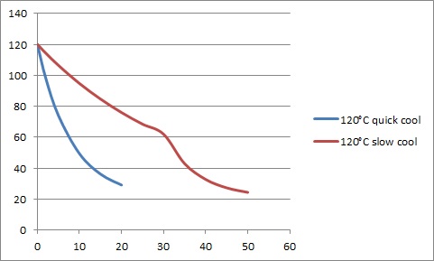
Quick and slow cooling from 120°C
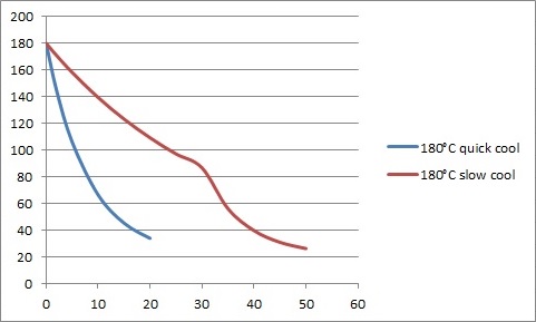
Quick and slow cooling from 180°C


Edge bead removal
Edge bead removal, or EBR, of PGMEA based UV resists on Spin Coater: Gamma E-beam and UV is done as a post-processing step on dry (soft baked) resist. The edge bead removal is thus done as a separate sequence run after the coating has finished. This limits the number of sequences needed on the tool, and also open up for edge bead removal of PGMEA based UV resist on wafers coated on other spin coaters.
Edge bead removal is done by spraying PGMEA onto the edge of the wafer through a special needle in order to dissolve the resist. The needle starts outside of the wafer, then moves onto the wafer and stays there for a thickness dependent time. 2µm AZ 5214E requires only 10s, while 10µm AZ 4562 requires 90s. After this time, the needle moves off the wafer again, and the wafer is spun at 2000 rpm for 10s in order to dry off the PGMEA. The spin speed during EBR depends on the size of the wafer, and backside rinse may be used during the EBR step.
Quality Control (QC)
| Quality Control (QC) for Spin Coater: Gamma e-beam & UV - AZ MiR 701 | ||||||||||||||||||||||||
Spin-off speed will be adjusted if film thickness is outside the limit. |
| Quality Control (QC) for Spin Coater: Gamma e-beam & UV - AR-P 6200.09 | ||||||||||||||||||||||||
Spin-off speed will be adjusted if film thickness is outside the limit. |
Standard Processes
HMDS priming
The standard HMDS priming process was developed (on Spin Coater: Gamma UV) to mimic the behavior of the IMTEC Star2000 HMDS oven, which produces a contact angle of 81-82° on an oxidized silicon surface. The fast HMDS priming was developed to have a process time of approximately one minute, in order to match the process time of typical coating and soft baking processes. General information on HMDS priming can be found here.
Sequence names, process parameters, and test results:
- (0201) DCH 50mm HMDS Standard
VPO temperature: 120°C
Process parameters: 30s vacuum bake @ -0.8 bar, HMDS injection, 90s reaction @ -0.3 bar, 10s evacuation after process, slow cooling @ 21°C.
- (0401) DCH 100mm HMDS Standard
- (0601) DCH 150mm HMDS Standard
VPO temperature: 120°C
Process parameters: 30s vacuum bake @ -0.8 bar, HMDS injection, 90s reaction @ -0.3 bar, 10s evacuation after process, quick cooling @ 21°C.
Test results:
| Substrate | Contact angle | Test date | Tester initials | Comments |
|---|---|---|---|---|
| Si with native oxide | ||||
- (0202) DCH 50mm HMDS Fast
VPO temperature: 120°C
Process parameters: 30s vacuum bake @ -0.8 bar, HMDS injection, 15s reaction @ -0.3 bar, 10s evacuation after process, slow cooling @ 21°C.
- (0402) DCH 100mm HMDS Fast
- (0602) DCH 150mm HMDS Fast
VPO temperature: 120°C
Process parameters: 30s vacuum bake @ -0.8 bar, HMDS injection, 15s reaction @ -0.3 bar, 10s evacuation after process, quick cooling @ 21°C.
Test results:
| Substrate | Contact angle | Test date | Tester initials | Comments |
|---|---|---|---|---|
| Si with native oxide | 76±1° | June 2017 | taran | Average of five measurements on one sample. A reference sample from Gamma UV measured the same. |
AZ 5214E coating
Coater2 (4" and 6")
Spin coating of standard thicknesses (1.5 - 3 µm) of AZ 5214E on Spin Coater: Gamma E-beam and UV Coater2 is divided into two or three steps: HMDS priming (optional), spin coating, and soft baking. The HMDS priming is equal to the HMDS fast process. Spin coating uses dynamic dispense of resist at 800 rpm, using a volume of 3 ml for 100 mm substrates, and 5 ml for 150 mm substrates, respectively. The dispense is followed by spin-off at a thickness dependent spin speed for 30 seconds. The wafer is decelerated at 1000 rpm/s before stopping. Soft baking is done at 90°C for 60s, and quick cooling is used.
In order to achieve thicker coatings of AZ 5214E while minimizing edge bead problems, a method of waiting before spin-off is used on Spin Coater: Gamma UV. The spin coating process consists of three steps: dispense, waiting, and spin-off. The first step is dynamic dispense of resist at 800 rpm, using a volume of 3 ml for 100 mm substrates, and 5 ml for 150 mm substrates, respectively. In the waiting step the resist is "dried" at low spin speed with low exhaust. The final spin-off step is short, but at relatively high spin speed, with backside rinse the first half of the time. Soft baking is done at 100°C for 90s in 1mm proximity. The coating may be affected by the backside rinse at the very edge of the wafer, something which should be considered if the resist is used as an etch mask.
Sequence names, process parameters, and test results:
- (4110) DCH 100mm 5214E 1.5um
- (4111) DCH 100mm 5214E 1.5um HMDS
Spin-off: 4900 rpm.
| Substrate | Thickness | Uniformity (+/-) | Test date | Tester initials | Comments |
|---|---|---|---|---|---|
| Silicon with native oxide | 1.52 µm | 0.36% | 20/3 2015 | taran | SAT result. 4" wafer, no HMDS. 5 wafers measured on Filmtek: thickness is average of all 5; uniformity is worst case. 9 points on each wafer, exclusion zone 5mm. |
| Silicon with native oxide | 1.52 µm | 0.59% | 13/11 2017 | taran | 4" wafer, with HMDS. 3 wafers measured on Filmtek: thickness is average of all 3; uniformity is worst case. 9 points on each wafer, exclusion zone 5mm. |
- (4120) DCH 100mm 5214E 2.2um
- (4121) DCH 100mm 5214E 2.2um HMDS
Spin-off: 2200 rpm.
| Substrate | Thickness | Uniformity (+/-) | Test date | Tester initials | Comments |
|---|---|---|---|---|---|
| Silicon with native oxide | 2.21 µm | 1.4% | 26/10 2017 | taran | 4" wafer, with HMDS. 3 wafers measured on Filmtek: thickness is average of all 3; uniformity is worst case. 9 points on each wafer, exclusion zone 5mm. |
- (4140) DCH 100mm 5214E 4.2um
- (4141) DCH 100mm 5214E 4.2um HMDS
Waiting: 60s @ 600 rpm. Spin-off: 10s @ 3500 rpm.
| Substrate | Thickness | Uniformity (+/-) | Test date | Tester initials | Comments |
|---|---|---|---|---|---|
| Silicon with native oxide | 4.22 µm | 0.8% | 13/11 2017 | taran | 4" wafer, with HMDS. 3 wafers measured on Filmtek: thickness is average of all 3; uniformity is worst case. 9 points on each wafer, exclusion zone 5mm. |
AZ MiR 701 (29cps) coating
Spin coating of standard thicknesses (1.3 - 2.5 µm) of AZ MiR 701 (29cps) on Spin Coater: Gamma e-beam & UV Coater2 is divided into two or three steps: HMDS priming (optional), spin coating, and soft baking. The HMDS priming is equal to the HMDS fast process. Spin coating uses dynamic dispense of resist at 800 rpm, using a volume of 3 ml for 100 mm substrates, and 5 ml for 150 mm substrates, respectively. The dispense is followed by spin-off at a thickness dependent spin speed for 30 seconds. The wafer is decelerated at 2000 rpm/s before stopping. Soft baking is done at 90°C for 60s. As MiR 701 has a tendency to produce "cotton candy" on the edges, soft baking is performed in 1 mm proximity.
In order to achieve thicker coatings of AZ MiR 701 (29cps) while minimizing edge bead problems, a method of waiting before spin-off is used on Spin Coater: Gamma E-beam & UV. The spin coating process consists of three steps: dispense, waiting, and spin-off. The first step is dynamic dispense of resist at 800 rpm, using a volume of 3 ml for 100 mm substrates, and 5 ml for 150 mm substrates, respectively. In the waiting step the resist is "dried" at low spin speed and low exhaust. The final spin-off step is short, but at relatively high spin speed, with backside rinse the first half of the time. Soft baking is done at 90°C for 90s. Contact baking is used since the backside is clean. The coating may be affected by the backside rinse at the very edge of the wafer, something which should be considered if the resist is used as an etch mask.
Sequence names, process parameters, and test results:
- (4210) DCH 100mm MiR 701 1.5um
- (4211) DCH 100mm MiR 701 1.5um HMDS see also QC
Spin-off: 4600 rpm.
| Substrate | Thickness | Uniformity (+/-) | Test date | Tester initials | Comments |
|---|---|---|---|---|---|
| Silicon with native oxide | 1.50 µm | 0.35% | 29/6 2017 | taran | SAT results. 4" wafer, no HMDS. 5 wafers measured on Filmtek: thickness is average of all 5; uniformity is worst case. 9 points on each wafer, exclusion zone 5mm. |
| Silicon with native oxide | 1.49 µm | 0.77% | 1/11 2017 | taran | 4" wafer, with HMDS. 3 wafers measured on Filmtek: thickness is average of all 3; uniformity is worst case. 9 points on one wafer, exclusion zone 5mm |
- (4220) DCH 100mm MiR 701 2um
- (4221) DCH 100mm MiR 701 2um HMDS
Spin-off: 2600 rpm.
| Substrate | Thickness | Uniformity (+/-) | Test date | Tester initials | Comments |
|---|---|---|---|---|---|
| Silicon with native oxide | 1.98 µm | 0.61% | 1/11 2017 | taran | 4" wafer, with HMDS. 3 wafers measured on Filmtek: thickness is average of all 3; uniformity is worst case. 9 points on one wafer, exclusion zone 5mm |
- (4240) DCH 100mm MiR 701 4um
- (4241) DCH 100mm MiR 701 4um HMDS
Waiting: 75s @ 600 rpm. Spin-off: 10s @ 3500 rpm.
| Substrate | Thickness | Uniformity (+/-) | Test date | Tester initials | Comments |
|---|---|---|---|---|---|
| Silicon with native oxide | 4.08 µm | 0.72% | 1/11 2017 | taran | 4" wafer, with HMDS. 3 wafers measured on Filmtek: thickness is average of all 3; uniformity is worst case. 9 points on one wafer, exclusion zone 5mm |
AR-P 6200 (CSAR) coating
Coater1 (2")
Spin coating of AR-P 6200.09 on Spin Coater: Gamma E-beam and UV Coater1 is divided into two steps: spin coating and soft baking. Spin coating uses dynamic dispense of resist at 1200 rpm, using a volume of 1 ml with the exhaust low during the dispense. The dispense is followed by spin-off at a thickness dependent spin speed for 60 seconds. Soft baking is done at 180°C in 1mm proximity for a thickness dependent time. Due to the high soft bake temperature, cooling is done in two steps: 30s in 1mm proximity followed by 20s in contact.
Sequence names, process parameters, and test results:
- (2318) DCH 50mm CSAR 180nm
Spin-off: 5400 rpm 60s, exhaust closed during dispense.
Soft bake: 180s @ 180°C, 1mm prox.
| Substrate | Thickness | Uniformity (±) | Test date | Tester initials | Comments |
|---|---|---|---|---|---|
| Silicon with native oxide | 179 nm | 0.28% | 30/6 2017 | taran | SAT result. 2" wafer. 2 wafers measured on Filmtek: thickness is average of both; uniformity is worst case. 5 points on each wafer, exclusion zone 3mm. |
| Silicon with native oxide | 183.4 nm | 0.29% | 7/11 2017 | taran | 2" wafer. 3 wafers measured on Filmtek: thickness is average all three; uniformity is worst case. 5 points on one wafer, exclusion zone 3mm. |
- (2325) DCH 50mm CSAR 250nm
Spin-off: 2800 rpm 60s, exhaust closed during dispense.
Soft bake: 180s @ 180°C, 1mm prox.
| Substrate | Thickness | Uniformity (±) | Test date | Tester initials | Comments |
|---|---|---|---|---|---|
| Silicon with native oxide | 251.0 nm | 0.33% | 7/11 2017 | taran | 2" wafer. 3 wafers measured on Filmtek: thickness is average all three; uniformity is worst case. 5 points on one wafer, exclusion zone 3mm. |
- (2351) DCH 50mm CSAR 500nm
Spin-off: 690 rpm 60s, exhaust closed during dispense.
Soft bake: 300s @ 180°C, 1mm prox.
| Substrate | Thickness | Uniformity (±) | Test date | Tester initials | Comments |
|---|---|---|---|---|---|
| Silicon with native oxide | 506.1 nm | 0.23% | 7/11 2017 | taran | 2" wafer. 3 wafers measured on Filmtek: thickness is average all three; uniformity is worst case. 5 points on one wafer, exclusion zone 3mm. |
Coater2 (4" and 6")
Spin coating of AR-P 6200.09 on Spin Coater: Gamma E-beam and UV Coater2 is divided into two steps: spin coating and soft baking. Spin coating uses dynamic dispense of resist at 1200 rpm with the exhaust low during the dispense, using a volume of 2 ml for 100 mm substrates, and 3 ml for 150 mm substrates, respectively. The dispense is followed by spin-off at a thickness dependent spin speed for 60 seconds. Soft baking is done at 180°C in 1mm proximity for a thickness dependent time. Due to the high soft bake temperature, cooling is done in two steps: 30s in 1mm proximity followed by 20s in contact.
Sequence names, process parameters, and test results:
- (4318) DCH 100mm CSAR 180nm
- (6318) DCH 150mm CSAR 180nm
Spin-off: 5200 rpm 60s, exhaust closed during dispense. [2021-06-30: Spin speed obsolete - JEHEM]
Spin-off: 4500 rpm 60s, exhaust closed during dispense. [2022-07-22: Spin speed obsolete - JEHEM]
Spin-off: 5496 rpm 60s, exhaust closed during dispense.
Soft bake: 180s @ 180°C, 1mm prox.
| Substrate | Thickness | Uniformity (±) | Test date | Tester initials | Comments |
|---|---|---|---|---|---|
| Silicon with native oxide | 178 nm | 0.5% | 23/6 2017 | taran | SAT result. 4" wafer. 6 wafers measured on Filmtek: thickness is average of all 6; uniformity is worst case. 9 points on each wafer, exclusion zone 5mm. |
| Silicon with native oxide | 179.2 nm | 0.39% | 16/11 2017 | taran | 4" wafer. 3 wafers measured on Filmtek: thickness is average of all 3; uniformity is worst case. 9 points on each wafer, exclusion zone 5mm. |
| Silicon dummy wafer | 183.1 nm | 0.32% | 29/05 2018 | taran | 6" wafer measured on Filmtek. 13 points, exclusion zone 5mm. |
| 100 mm Silicon dummy wafer | 180.5 nm | 0.1% | 2021-06-30 | JEHEM | 100 mm wafer measured on ellipsometer VASE. 9 points, exclusion zone 10 mm. |
| 150 mm Silicon dummy wafer | 180.9 nm | 0.5% | 2021-06-30 | JEHEM | 150 mm wafer measured on ellipsometer VASE. 13 points, exclusion zone 5 mm. |
- (4325) DCH 100mm CSAR 250nm see also QC
- (6325) DCH 150mm CSAR 250nm
Spin-off: 2600 rpm 60s, exhaust closed during dispense. [2021-06-30: Spin speed obsolete - JEHEM]
Spin-off: 2300 rpm 60s, exhaust closed during dispense. [2022-07-22: Spin speed obsolete - JEHEM]
Spin-off: 2875 rpm 60s, exhaust closed during dispense.
Soft bake: 180s @ 180°C, 1mm prox.
| Substrate | Thickness | Uniformity (±) | Test date | Tester initials | Comments |
|---|---|---|---|---|---|
| Silicon with native oxide | 250.7 nm | 0.93% | 16/11 2017 | taran | 4" wafer. 3 wafers measured on Filmtek: thickness is average of all 3; uniformity is worst case. 9 points on each wafer, exclusion zone 5mm. |
| 100 mm Silicon dummy wafer | 247.0 nm | 0.1% | 2021-06-30 | JEHEM | 100 mm wafer measured on ellipsometer VASE. 9 points, exclusion zone 10 mm. |
| 150 mm Silicon dummy wafer | 249.7 nm | 0.8% | 2021-06-30 | JEHEM | 150 mm wafer measured on ellipsometer VASE. 13 points, exclusion zone 5 mm. |
- (4351) DCH 100mm CSAR 500nm
Spin-off: 650 rpm 60s, exhaust closed during dispense. [2021-06-30: Spin speed obsolete - JEHEM]
Spin-off: 560 rpm 60s, exhaust closed during dispense. [2022-07-22: Spin speed obsolete - JEHEM]
Spin-off: 733 rpm 60s, exhaust closed during dispense.
Soft bake: 180s @ 180°C, 1mm prox.
| Substrate | Thickness | Uniformity (±) | Test date | Tester initials | Comments |
|---|---|---|---|---|---|
| Silicon with native oxide | 502 nm | 0.75% | 16/11 2017 | taran | 4" wafer measured on Filmtek. 9 points, exclusion zone 5mm. |
| 100 mm Silicon dummy wafer | 505.6 nm | 1.1% | 2021-06-30 | JEHEM | 100 mm wafer measured on ellipsometer VASE. 9 points, exclusion zone 10 mm. |
AZ 4562 coating
Spin coating of standard thicknesses (5 - 10 µm) of AZ 4562 on Spin Coater: Gamma E-beam and UV Coater2 is divided into two steps: Spin coating, and soft baking. The spin coating uses dynamic dispense of resist at 300 rpm, using a volume of 3 ml for 100 mm substrates, and 6 ml for 150 mm substrates, respectively. The dispense is followed by spin-off at a thickness dependent spin speed for 30 seconds with backside rinse. The wafer dried at 800 rpm for 15s before stopping. Soft baking is done at 100°C in 1 mm proximity for 300s. The coating may be affected by the backside rinse at the very edge of the wafer, something which should be considered if the resist is used as an etch mask.
In order to achieve thicker coatings of AZ 4562 while minimizing edge bead problems, a method of short spin-off is used on Spin Coater: Gamma E-beam & UV. The spin coating process consists of three steps: dispense, spin-off, and waiting. The first step is dynamic dispense of resist at 300 rpm, using a volume of 3 ml for 100 mm substrates, and 5 ml for 150 mm substrates, respectively. The spin-off step is short, but at moderate spin speed. In the waiting step the resist is "leveled" at 0 rpm for 60s. Soft baking is done at 100°C, 1mm proximity for 600s.
Sequence names, process parameters, and test results:
- (4462) DCH 100mm 4562 6.2um
Spin-off: 5000 rpm
| Substrate | Thickness | Uniformity (+/-) | Test date | Tester initials | Comments |
|---|---|---|---|---|---|
| Silicon with native oxide | 6.19 µm | 1.44% | 1/11 2017 | taran | 4" wafer. 3 wafers measured on Filmtek: thickness is average of all 3; uniformity is worst case. 9 points on each wafer, exclusion zone 5mm. |
- (4410) DCH 100mm 4562 10um
Spin-off: 2000 rpm
| Substrate | Thickness | Uniformity (+/-) | Test date | Tester initials | Comments |
|---|---|---|---|---|---|
| Silicon with native oxide | 10.18 µm | 1.24% | 1/11 2017 | taran | 4" wafer. 3 wafers measured on Filmtek: thickness is average of all 3; uniformity is worst case. 9 points on each wafer, exclusion zone 5mm. |
- (4415) 100mm 4562 15um
- (6415) 150mm 4562 15um
Spin-off: 10s @ 2000 rpm. Soft bake: 600s @ 100°C, 1mm proximity
| Substrate | Thickness | Uniformity (+/-) | Test date | Tester initials | Comments |
|---|---|---|---|---|---|
| Silicon with native oxide | 14.4 µm | 2.4% | 27/11 2019 | taran | 4" wafer measured on Filmtek: 9 points, exclusion zone 5mm. |
| Silicon with native oxide | 15.5 µm | 1.0% | 28/09 2020 | taran | 6" wafer measured on Filmtek: 13 points, exclusion zone 7mm. |
- (4420) DCH 100mm 4562 20um
Spin-off: 6s @ 2000 rpm. Soft bake: 600s @ 100°C, 1mm proximity
| Substrate | Thickness | Uniformity (+/-) | Test date | Tester initials | Comments |
|---|---|---|---|---|---|
| Silicon with native oxide | 18.63 µm | 1.0% | 1/11 2017 | taran | 4" wafer. 2 wafers measured on Filmtek: thickness is average of both; uniformity is worst case. 9 points on each wafer, exclusion zone 5mm. |
Edge bead removal
Edge bead removal, or EBR, of PGMEA based UV resists on Spin Coater: Gamma E-beam and UV is done as a post-processing step on dry (soft baked) resist. The edge bead removal is thus done as a separate sequence run after the coating has finished. This limits the number of sequences needed on the tool, and also open up for edge bead removal of PGMEA based UV resist on wafers coated on other spin coaters.
Edge bead removal is done by spraying PGMEA onto the edge of the wafer through a special needle in order to dissolve the resist. The needle starts outside of the wafer, then moves onto the wafer and stays there for a thickness dependent time. 2µm AZ 5214E requires only 10s, while 10µm AZ 4562 requires 90s. After this time, the needle moves off the wafer again, and the wafer is spun at 2000 rpm for 10s in order to dry off the PGMEA. The spin speed during EBR depends on the size of the wafer, and backside rinse may be used during the EBR step.
Coater1 (2")
Sequence names and process parameters:
- (2531) DCH 2in EBR 3mm 10s
- (2532) DCH 2in EBR 3mm 20s
- (2534) DCH 2in EBR 3mm 40s
- (2536) DCH 2in EBR 3mm 60s
- (2539) DCH 2in EBR 3mm 90s
1000 rpm during EBR, no BSR.
Coater2 (4" and 6")
Sequence names and process parameters:
- (4541) DCH 100mm EBR 4mm 10s
- (4542) DCH 100mm EBR 4mm 20s
- (4544) DCH 100mm EBR 4mm 40s
- (4546) DCH 100mm EBR 4mm 60s
- (4549) DCH 100mm EBR 4mm 90s
500 rpm during EBR, BSR during EBR.
- (6571) DCH 150mm EBR 7mm 10s
- (6572) DCH 150mm EBR 7mm 20s
- (6574) DCH 150mm EBR 7mm 40s
- (6576) DCH 150mm EBR 7mm 60s
- (6579) DCH 150mm EBR 7mm 90s
500 rpm during EBR, BSR during EBR.
Syringe Processes
Use of the syringe requires special training, and would as a starting point require batch processing of many wafers. It is not an easy process to setup, and is not intended for processing a few wafers now and then.
The syringe sequences on Spin Coater: Gamma E-beam and UV Coater1 are designed with anisole based e-beam resist in mind. Processing is divided into two steps: spin coating and soft baking. Spin coating uses dynamic dispense of resist at 1000 rpm, using the Fishman syringe program number 1 (the dispense step is designed for ~0.75 cc at 1 cc per sec). The dispense is followed by spin-off at a sequence dependent spin speed for 60 seconds. Soft baking is done at 180°C for 180s in 1mm proximity, and slow cooling is used. Due to the high soft bake temperature, cooling is done in two steps: 30s in 1mm proximity followed by 20s in contact.
Sequence names:
- (2205) DCH 50mm Fishman 500rpm 60s
- (2210) DCH 50mm Fishman 1000rpm 60s
- (2215) DCH 50mm Fishman 1500rpm 60s
- (2220) DCH 50mm Fishman 2000rpm 60s
- (2230) DCH 50mm Fishman 3000rpm 60s
- (2240) DCH 50mm Fishman 4000rpm 60s
- (2250) DCH 50mm Fishman 5000rpm 60s
- (2260) DCH 50mm Fishman 6000rpm 60s