Jump to content

Specific Process Knowledge/Lithography/Strip: Difference between revisions

From LabAdviser
Tigre (talk | contribs)
Created page with "==Plasma asher 1 - ''All purpose''== 322 × 324px|thumb|The PlasmaAsher1 is placed in Cleanroom 3. The Plasma Asher1( 300 auto load model) can be u..."
 
Jehem (talk | contribs)
 
(294 intermediate revisions by 11 users not shown)
Line 1: Line 1:
==Plasma asher 1 - ''All purpose''==
{{cc-nanolab}}
[[Image:plasmaasher2.JPG|322 × 324px|thumb|The PlasmaAsher1 is placed in Cleanroom 3.]]


The Plasma Asher1( 300 auto load model) can be used for the following process:
'''Feedback to this page''': '''[mailto:labadviser@nanolab.dtu.dk?Subject=Feed%20back%20from%20page%20http://labadviser.nanolab.dtu.dk/index.php?title=Specific_Process_Knowledge/Lithography/Strip click here]'''


*Photoresist stripping
[[Category: Equipment|Lithography strip]]
*Surface cleaning after storage
[[Category: Lithography|Strip]]
*Surface cleaning after processes using oil pump or diffusion pump vacuum
*Surface cleaning as part of photolithography after wet developing of lacquer structures prior to wet or plasma etching
*Stripping of photoresist layers after etching, including after being exposed to high temperatures as after implantation, ion etching, sputter etching, RIE
*Removal of organic passivating layers and masks
*Etching of glass and ceramic
*Etching of SiO<math>_2</math>, Si<math>_3</math>N<math>_4</math>, Si
*Removal of polyimide layers


The machine can be used for almost every materials, but if you have any doubt about your materials are compatible with the plasma process it is better to ask photolithography group at Danchip.
__TOC__


= Strip Comparison Table =
{| class="wikitable"
|-
!
! [[Specific_Process_Knowledge/Lithography/Strip#Plasma Asher 3: Descum|Plasma Asher 3: Descum]]
! [[Specific_Process_Knowledge/Lithography/Strip#Plasma_Asher_4|Plasma Asher 4 (Clean)]]
! [[Specific_Process_Knowledge/Lithography/Strip#Plasma Asher 5|Plasma Asher 5 (Dirty)]]
! [[Specific_Process_Knowledge/Lithography/Strip#Resist Strip|Resist strip]]
! [[Specific Process Knowledge/Lithography/LiftOff|Lift-off]]
|-
! scope=row style="text-align: left;" |  Purpose
| Resist descum
|
*Resist stripping
*Resist descum
|
*Resist stripping
*Resist descum
| Resist stripping
| Metal lift-off
|-
! scope=row style="text-align: left;" | Method
| Plasma ashing
| Plasma ashing
| Plasma ashing
| Solvent & ultrasonication
| Solvent & ultrasonication
|-
! scope=row style="text-align: left;" | Process gasses
| O<sub>2</sub> (50 sccm)
|
*O<sub>2</sub> (0-500 sccm)
*<sub>2</sub> (0-500 sccm)
|
*O<sub>2</sub> (0-500 sccm)
*N<sub>2</sub> (0-500 sccm)
*CF<sub>4</sub> (0-200 sccm)
| NA
| NA
|-
! scope=row style="text-align: left;" | Process power
| 10-100 W (10-100%)
| 150-1000 W
| 150-1000 W
| NA
| NA
|-
! scope=row style="text-align: left;" | Process solvent
| NA
| NA
| NA
|
*NMP (Remover 1165)
*IPA (rinsing agent)
|
*NMP (Remover 1165)
*IPA (rinsing agent)
|-
! scope=row style="text-align: left;" | Substrate batch
|
*Chips: several
*50 mm wafer: several
*100 mm wafer: 1
|
*Chips: several
*50 mm wafer: several
*100 mm wafer: 1-25
*150 mm wafer: 1-25
*200 mm wafer: 1-25
|
*Chips: several
*50 mm wafer: several
*100 mm wafer: 1-25
*150 mm wafer: 1-25
*200 mm wafer: 1-25
|
*100 mm wafer: 1-25
*150 mm wafer: 1-25
|
*100 mm wafer: 1-25
*150 mm wafer: 1-25
|-
! scope=row style="text-align: left;" | Substrate materials
|
*<span style="color:red">'''No polymer substrates'''</span><br>
*Silicon substrates
*III-V substrates
*Glass substrates
*Films, or patterned films, of any material except type IV (Pb, Te)
|
*<span style="color:red">'''No metals'''</span><br>
*<span style="color:red">'''No metal oxides'''</span><br>
*<span style="color:red">'''No III-V materials'''</span><br>
*Silicon substrates
*Glass substrates
*Polymer substrates
*Films, or patterned films, of resists/polymers
|
*Silicon substrates
*III-V substrates
*Glass substrates
*Polymer substrates
*Films, or patterned films, of any material except type IV (Pb, Te)
|
*<span style="color:red">'''No metals'''</span><br>
*<span style="color:red">'''No metal oxides'''</span><br>
*Silicon substrates
*III-V substrates
*Glass substrates
*Polymer substrates
*Films, or patterned films, of resists/polymers
|
*Silicon substrates
*III-V substrates (only if clean)
*Glass substrates
*Films, or patterned films, of any material except type IV (Pb, Te)
|}


===Overview of typical processes===
<br clear="all" />


{| border="2" cellspacing="0" cellpadding="4" align="left"
= Plasma Ashing process parameters=
!
 
! Photoresist stripping
{| class="wikitable"
! Surface treatment of plastic, ceramic and metal
! Ashing of organic material
|-
|'''Process pressure'''
|0.8- 1.0mbar
|0.5- 1.0mbar
|0.8-1.5mbar
|-
|-
|'''Process gases'''
!  !! [[Specific_Process_Knowledge/Lithography/Strip#Plasma_Asher_4|Resist stripping (PA4 & PA5)]] !! [[Specific_Process_Knowledge/Lithography/Descum#Plasma_Asher_3:_Descum|Descum (PA3)]] !! [[Specific_Process_Knowledge/Lithography/Descum#Plasma_Asher_4|Descum (PA4 & PA5)]] !! Surface treatment !! Other ashing of organic material
|O<sub>2</sub>, N<sub>2</sub>
|O<math>_2</math>, CF<math>_4</math>, N<math>_2</math> or their mixtures
|O<sub>2</sub>
|-
|-
|'''Process power'''
! scope=row style="text-align: left;" | Process pressure
|600-1000W
| 1.3 mbar || 0.8 mbar || 1.3 mbar || 0.5-1.5 mbar || 0.5-1.5 mbar
|150-300W
|1000W or less for heat- sensitive materials
|-
|-
|'''Process time'''
! scope=row style="text-align: left;" | Process gasses
|5-60min, depending of photoresist thickness
|
|a few seconds to a few minutes
*O<sub>2</sub> (100 sccm)
|Between 0.5 and 20 hours, depending on the material
*N<sub>2</sub> (100 sccm)
|
*O<sub>2</sub> (45 sccm)
|
*O<sub>2</sub> (100 sccm)
*N<sub>2</sub> (100 sccm)
|
*O<sub>2</sub>
*N<sub>2</sub>
*CF<sub>4</sub>
|
*O<sub>2</sub>
|-
|-
|'''Batch size'''
! scope=row style="text-align: left;" | Process power
|1-10 wafers at a time
| 1000 W || 100 W || 200 W || 150-1000 W || 150-1000 W
|1 wafer at a time
|1 wafer at a time, use a container: Petri dish, evaporating dish weighing dish, beaker, etc.
|-
|-
|'''Size of substrate'''
! scope=row style="text-align: left;" | Process time
|2"-6"
| 20-90 minutes || 1-10 minutes || 5-15 minutes || Seconds to minutes || Many hours, material dependent
|2"-6"
|2"-6"
|-
|-
|'''Allowed materials'''
! scope=row style="text-align: left;" | Substrate batch
|All
| 1-25 || 1-2 || 1-25 || 1 || 1
|All
|}
|All
 
<br clear="all" />


|-
=Plasma Asher 1=
|}
<span style="color:red">Plasma asher 1 was decommissioned 2024-12-02.</span>
 
[[Specific Process Knowledge/Lithography/Strip/PlasmaAsher1|Information about decommissioned tool can be found here.]]
<br clear="all" />
 
=Plasma Asher 2=
<span style="color:red">Plasma asher 2 was decommissioned 2024-12-02.</span>


[[Specific Process Knowledge/Lithography/Strip/PlasmaAsher2|Information about decommissioned tool can be found here.]]
<br clear="all" />
<br clear="all" />


=Plasma Asher 3: Descum=
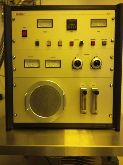
[[image:2017-03-15 13.12.45.jpg|400px|thumb|Plasma Asher 3: Descum is a low power plasma asher dedicated for descumming on smaller substrates.]]
Product name: Diener Pico Plasma Asher<br>
Year of purchase: 2014
The Plasma Asher 3: Descum is dedicated for resist descum, i.e. removal of remains resist traces after development. It has a small chamber, so you can only load a single 100 mm substrate, or a few smaller pieces.
In this machine, only Oxygen is used for processing.


<b>Typical process parameters:</b><br>
Process: Photoresist descumming<br>
Pressure: 0.2-0.8 mbar<br>
Gas: 45 sccm O<sub>2</sub><br>
Power: 100 W (100%)<br>
Time: 1 -10 minutes (depending on photoresist type and thickness)<br>


Other materials have not been tested.


A typical process time for stripping of 1.5 µm AZ5214e resist is 15-25 min and for stripping of 9.5 µm AZ4562 resist is 20-35 min with the process parameters: 210ml O<math>_2</math>/min or mixture of 210ml O<math>_2</math>/min and 70ml N<math>_2</math>/min, power 1000W.
The user manual, user APV, and contact information can be found in [http://labmanager.dtu.dk/function.php?module=Machine&view=view&mach=423 LabManager] - '''requires login'''


==Plasma asher 2 - ''Clean/no metals''==
===Process Information===
[[Image:Plasma_Asher_6inch.jpg|300x300px|thumb|Plasma asher for removing AZ resist on 6" wafers: positioned in cleanroom ? (class 10 yellow room)]]
Detailed information about descum processing on Plasma asher 3: Descum can be found [[Specific Process Knowledge/Lithography/Descum|here]].


The Plasma Asher 2 is the same as Plasma Asher 1 but has another loading system which is more convenient for batch loading of 6inch substrates.
<br clear="all" />


In this machine, only O2 and N2 gases are used for processes (in PlasmaAsher1, CF4 is used as well).
=Plasma Asher 4=
[[File:PA5 front.jpg|400px|thumb|Plasma asher 4 in cleanroom E-5.|right]]
Product name: PVA Tepla Gigabatch 380M<br>
Year of purchase: 2024


The typical process parameters when operating the equipment:
The Plasma Asher 4 can be used for the following processes:
*Photeresist stripping
*Photoresist stripping
Pressure: 0.8 - 1.0 mbar
*Descumming
*Surface cleaning
*Removal of organic passivation layers and masks


Gas: O2


Power: 600 - 1000 watts
Plasma asher 4 has the following material restrictions:
*No metals allowed
*No metal oxides allowed
*No III-V materials allowed


Time: 5 -30 min., depending on photoresist type and thickness
The user manual, risk assessment, and contact information can be found in [http://labmanager.dtu.dk/function.php?module=Machine&view=view&mach=530 LabManager] - '''requires login'''


A typical process time for stripping of 1.5 um AZ5214e resist is 25 min for 6 wafers load in a boat, recipe 1.  
'''Typical stripping parameters'''<br>
Tested with 1.5 µm AZ 5214E on 100 mm silicon substrate.
*O<sub>2</sub>: 100 sccm
*N<sub>2</sub>: 100 sccm
*Pressure (DSC): 1.3 mbar
*Power: 1000 W
*Time (single wafer): 20-30 minutes
*Time (full boat): 90 minutes


A Descum process in manuel mode:O2:70, N2:70, power:150W, time:10min Be sure to wait for cooling if the mashine has been used at 1000W right before.
<br clear="all" />
At a load at 2 Fused silicawafers resist removed 0.01-01,5um


The other materials have not been tested yet.
==Process gas ratio for plasma asher 4 & 5==
[[File:PA_gas_mix_v3.png|400px|thumb|Ashing rate as function of gas mix ratio when processing a single 100 mm wafer and when processing a full boat with 25 wafers. The green area (~50% N<sub>2</sub>) covers the optimum range for both situations.|right]]
The ashing rate is related to the gas mix, usually expressed as percentage of nitrogen of the total amount of gas. Process development tests found that a gas mix of 50% nitrogen gives the highest ashing rate for both processing single substrates and when processing a full boat with 25 substrates.  


==Acetone strip with ultrasound==
Please note that the ashing rate for a full boat is approximately ten times slower, than the processing time for a single substrate.
{| border="1" cellspacing="0" cellpadding="4" align="right"
 
|[[Image:Acetone_rough.jpg|150x150px|thumb|Acetone bath "rough" for removing most of the resist]]
{| class="wikitable"
|[[Image:Acetone_fine.jpg|150x150px|thumb|Acetone bath "fine" for removing the rest of the resist incl. ultrasound]]
|-
|-
!  !! Single substrate !! Full boat
|-
! scope=row style="text-align: left;" | Test results
| Highest ashing rate at 30-80% Nitrogen || Highest ashing rate at 50-70% Nitrogen
|-
! scope=row style="text-align: left;" | Wafers
| 1 || 25
|-
! scope=row style="text-align: left;" | Wafer size
| 100 mm || 100 mm
|-
! scope=row style="text-align: left;" | Boat position
| Center of chamber || Center of chamber
|-
! scope=row style="text-align: left;" | Test wafer position
| Center of boat || Center of boat
|-
! scope=row style="text-align: left;" | Total gas flow rate
| 500 sccm || 200 sccm
|-
! scope=row style="text-align: left;" | Gas mix ratio
| Tested parameter || Tested parameter
|-
! scope=row style="text-align: left;" | Chamber pressure
| 1.25 mbar || 1.3 mbar
|-
! scope=row style="text-align: left;" | Power
| 1000 W || 1000 W
|-
! scope=row style="text-align: left;" | Test processing time
| 2 minutes || 10 minutes
|-
! scope=row style="text-align: left;" | Test average temperature
| 43°C || 47°C
|}
|}


This acetone strip is only for wafers without metal and SU-8!
<br clear="all" />


There is two acetone bath: one rough for stripping the most of the resist from the surface and one fine with a ultrasound for cleaning the  resists remains.
==Process chamber pressure for plasma asher 4 & 5==
[[File:PA_chamber_pressure_v3.png|400px|thumb|Ashing rate as function of chamber pressure when processing a single substrate and when processing a full boat with 25 substrates. The green area covers the optimum range (~1.3 mbar) for both situations.|right]]
The ashing rate is related to the chamber pressure during processing. Process development tests found that 1.3 mbar gives the highest ashing rate for both processing single substrates and when processing a full boat with 25 substrates.  


Please note that the ashing rate for a full boat is approximately ten times slower, than the processing time for a single substrate.


'''Here are the main rules for acetone strip use:'''
{| class="wikitable"
*Place the wafers in a wafer holder and put them in the first bath for 2-5 min, this time is depending how much resist you have on the surface.
|-
*After the rough strip place your wafers directly in the final bath, switch on for the ultra sound  and strip them for 2-3 min.
!  !! Single substrate !! Full boat
*Rinse your wafers for 4-5 min. in running water after stripping .
|-
! scope=row style="text-align: left;" | Test results
| Highest ashing rate at 1.3 mbar || Highest ashing rate at 1.4 mbar
|-
! scope=row style="text-align: left;" | Wafers
| 1 || 25
|-
! scope=row style="text-align: left;" | Wafer size
| 100 mm || 100 mm
|-
! scope=row style="text-align: left;" | Boat position
| Center of chamber || Center of chamber
|-
! scope=row style="text-align: left;" | Test wafer position
| Center of boat || Center of boat
|-
! scope=row style="text-align: left;" | Total gas flow rate
| 150 sccm || 200 sccm
|-
! scope=row style="text-align: left;" | Gas mix ratio
| 30% N<sub>2</sub> || 50% N<sub>2</sub>
|-
! scope=row style="text-align: left;" | Chamber pressure
| Tested parameter || Tested parameter
|-
! scope=row style="text-align: left;" | Power
| 1000 W || 1000 W
|-
! scope=row style="text-align: left;" | Test processing time
| 2 minutes || 10 minutes
|-
! scope=row style="text-align: left;" | Test average temperature
| 43°C || 55°C
|}


<br clear="all" />
<br clear="all" />


==Lift-off wet bench==
==Process gas flow rate for plasma asher 4 & 5==
[[Image:Acetone_lift-off.jpg|300x300px|thumb|Acetone lift-off: positioned in cleanroom 3]]
[[File:PA_flowRate_v4.png|400px|thumb|Ashing rate as function of total gas flow when processing a single substrate and when processing a full boat with 25 wafers. The green area covers the optimum range (~200 sccm) for both situations.|right]]
This bench is only for wafers with metal!
The ashing rate is related to the total gas flow rate during processing. Process development tests found that 200 sccm gives the highest ashing rate for both processing single substrates and when processing a full boat with 25 substrates. The experiments indicate that the gas flow rate has only a minor impact on the ashing rate.


Here are the main rules for lift-off bench use:
Please note that the ashing rate for a full boat is approximately ten times slower, than the processing time for a single substrate.
*Place the wafers in a dedicated wafer holder.
 
*Put the holder in the acetone and start the ultrasound. The strip off time is depending of resist thickness.
{| class="wikitable"
*Rinse your wafers for 4-5 min. in running water after stripping.
|-
!  !! Single substrate !! Full boat
|-
! scope=row style="text-align: left;" | Test results
| Highest ashing rate at 200 sccm || Highest ashing rate at 200 sccm
|-
! scope=row style="text-align: left;" | Wafers
| 1 || 25
|-
! scope=row style="text-align: left;" | Wafer size
| 100 mm || 100 mm
|-
! scope=row style="text-align: left;" | Boat position
| Center of chamber || Center of chamber
|-
! scope=row style="text-align: left;" | Test wafer position
| Center of boat || Center of boat
|-
! scope=row style="text-align: left;" | Total gas flow rate
| Tested parameter || Tested parameter
|-
! scope=row style="text-align: left;" | Gas mix ratio
| 30% N<sub>2</sub> || 30% N<sub>2</sub>
|-
! scope=row style="text-align: left;" | Chamber pressure
| 1.3 mbar || 1.3 mbar
|-
! scope=row style="text-align: left;" | Power
| 1000 W || 1000 W
|-
! scope=row style="text-align: left;" | Test processing time
| 2 minutes || 10 minutes
|-
! scope=row style="text-align: left;" | Test average temperature
| 43°C || 47°C
|}


Find more info about the lift-off process here: [[Specific Process Knowledge/Photolithography/AZ5214E standard resist - reverse process]]
<br clear="all" />
<br clear="all" />


==Overview of acetone benches==
==Process power for plasma asher 4 & 5==
[[File:PA_power_v3.png|400px|thumb|Ashing rate as function of microwave power.|right]]
The ashing rate is related to the power used during processing. Higher power increases ashing rate.


{| border="2" cellspacing="0" cellpadding="4" align="left"
{| class="wikitable"
!  
|-
! Acetone strip
!  !! Single substrate
! Lift-off
|-
|-  
! scope=row style="text-align: left;" | Test results
|'''General description'''
| Ashing rate follows Power
|
|-
wet stripping of resist
! scope=row style="text-align: left;" | Wafers
|
| 1
lift-off process
|-
! scope=row style="text-align: left;" | Wafer size
| 100 mm
|-
! scope=row style="text-align: left;" | Boat position
| Center of chamber
|-
! scope=row style="text-align: left;" | Test wafer position
| Center of boat
|-
! scope=row style="text-align: left;" | Total gas flow rate
| 200 sccm
|-
! scope=row style="text-align: left;" | Gas mix ratio
| 30% N<sub>2</sub>
|-
! scope=row style="text-align: left;" | Chamber pressure
| 1.3 mbar
|-
! scope=row style="text-align: left;" | Power
| Tested parameter
|-
|-
|'''Chemical solution'''
! scope=row style="text-align: left;" | Test processing time
|CH<sub>3</sub>COCH<sub>3</sub>
| 2 minutes
|CH<sub>3</sub>COCH<sub>3</sub>
|-
|-
|'''Process temperature'''
! scope=row style="text-align: left;" | Test average temperature
|20 <sup>o</sup>C
| 40°C
|}


|20 <sup>o</sup>C
<br clear="all" />


==Process temperature for plasma asher 4 & 5==
[[File:PA_temperature_v2.png|400px|thumb|Ashing rate as function of temperature.|right]]
The ashing rate is related to the temperature during processing. Higher temperature increases ashing rate.
{| class="wikitable"
|-
|-
!  !! Single substrate
|-
! scope=row style="text-align: left;" | Test results
| Ashing rate follows temperature
|-
! scope=row style="text-align: left;" | Wafers
| 1
|-
! scope=row style="text-align: left;" | Wafer size
| 100 mm
|-
! scope=row style="text-align: left;" | Boat position
| Center of chamber
|-
! scope=row style="text-align: left;" | Test wafer position
| Center of boat
|-
! scope=row style="text-align: left;" | Total gas flow rate
| 200 sccm
|-
! scope=row style="text-align: left;" | Gas mix ratio
| 30% N<sub>2</sub>
|-
! scope=row style="text-align: left;" | Chamber pressure
| 1.3 mbar
|-
! scope=row style="text-align: left;" | Power
| 1000 W
|-
! scope=row style="text-align: left;" | Test processing time
| 2 minutes
|-
! scope=row style="text-align: left;" | Test average temperature
| Tested parameter
|}
<br clear="all" />
==Comparison of ashing rate between substrate sizes for plasma asher 4 & 5==
[[File:PA_comparison_v3.png|400px|thumb|Comparison of ashing rate with different substrate sizes. Process was done using a single substrate placed in the middle of the glass boat, which was placed in the center of the chamber.|right]]
The ashing rate is highest for 100 mm substrates, lower for 150 mm substrates and even lower for 200 mm substrates.
All substrate sizes follows the same pattern:
*Ashing rate increases with a higher percentage nitrogen in the gas mix
*Ashing rate increases with a higher chamber pressure
*The total gas flow has only little influence on the ashing rate, but <i>slightly</i> favors the lower flow rate of 200 sccm, similar to previous experiment results


|'''Batch size'''
<br clear="all" />
|
 
1-25 wafers at a time
'''Process parameter impact on ashing rate'''<br>
|
Investigating the ashing rate using linear regression models on the process parameters, indicates that the gas mix and the chamber pressure has a significant impact on the ashing rate, while the gas flow has only little effect:
1-25 wafer at a time
<gallery mode="packed-hover" heights="150">
ParamEffect_100_mm_v1.png|100 mm parameter impact
ParamEffect_150_mm_v1.png|150 mm parameter impact
ParamEffect_200_mm_v1.png|200 mm parameter impact
</gallery>
 
<br clear="all" />
 
=Plasma Asher 5=
[[File:PA5 front.jpg|400px|thumb|Plasma asher 5 in cleanroom E-5.|right]]
Product name: PVA Tepla Gigabatch 380M<br>
Year of purchase: 2024
 
The Plasma Asher 5 can be used for the following processes:
*Photoresist stripping
*Descumming
*Surface cleaning
*Removal of organic passivation layers and masks
 
 
Furthermore plasma processing using CF<sub>4</sub> in plasma asher 5 can be used for:
*Etching of glass and ceramic
*Etching of SiO<sub>2</sub>, Si<sub>3</sub>N<sub>4</sub>, Si
*Removal of polyimide layers
 
 
Plasma asher 5 can be used for almost every material, but if you have any doubt if your materials are compatible/allowed in plasma asher 5, feel free to ask the lithography group at Nanolab.
 
The user manual, risk assessment, and contact information can be found in [http://labmanager.dtu.dk/function.php?module=Machine&view=view&mach=531 LabManager] - '''requires login'''
 
===Process Information===
Plasma asher 5 is identical to plasma asher 4, see resist strip processing for plasma asher 4 [[Specific_Process_Knowledge/Lithography/Strip#Plasma_Asher_4|here]].
 
 
'''Processes specifically only for plasma asher 5:'''<br>
*[[Specific Process Knowledge/Etch/Etching of Silicon Oxide/SiO2 etch using Plasma Asher |SiO<sub>2</sub> etch using Plasma Asher 1]]
*[[Specific Process Knowledge/Lithography/Descum#Plasma Asher 5|Descum using plasma asher 5]]
 
<br clear="all" />
 
=Resist Strip=
[[Image:Resist_strip.jpg|400px|thumb|Resist strip bench in D-3]]
 
This resist strip is only for wafers without metal and SU-8.
 
There are one Remover 1165 bath for stripping and one IPA bath for rinsing.
 
'''Here are the main rules for resist strip use:'''
*Place the wafers in a wafer holder and put them in the first bath for 10 min, this time is depending how much resist you have on the surface.
*After the strip rinse your wafers in the IPA bath for 2-3 min.
*Rinse your wafers for 4-5 min. in running water after stripping.
 
 
The user manual and contact information can be found in LabManager: [http://labmanager.dtu.dk/function.php?module=Machine&view=view&mach=385 Resist Strip] - '''requires login'''
 
<br clear="all" />
 
==Overview of wet bench 06 and 07==
{| class="wikitable"
|-
!  !! [[Specific Process Knowledge/Lithography/Strip#Resist_Strip|Resist Strip]]  !! [[Specific Process Knowledge/Lithography/LiftOff#Lift-off_wet_bench_07|Lift-off]]
|-
! scope=row style="text-align: left;" | Process
| Wet resist strip || Metal lift-off process
|-
! scope=row style="text-align: left;" | Chemical
| Remover 1165 (NMP) || Remover 1165 (NMP)
|-
! scope=row style="text-align: left;" | Process temperature
| Up to 65°C || Up to 65°C
|-
! scope=row style="text-align: left;" | Substrate batch
| 1-25 wafers || 1-25 wafers
|-
|-
|'''Size of substrate'''
! scope=row style="text-align: left;" | Substrate size
|
*100 mm wafers
*150 mm wafers
|
|
4" wafers
*100 mm wafers
|
*150 mm wafers
4" wafers
|-
|-
|'''Allowed materials'''
! scope=row style="text-align: left;" | Materials allowed
|
|  
*Silicon
*Silicon
*Silicon Oxide
*Silicon oxide
*Silicon Nitride
*Silicon nitride
*Silicon Oxynitride
*Silicon oxynitride
| All metals except Type IV (Pb, Te)
|}


|
<br clear="all" />
*All metals
 
|-
|}

Latest revision as of 11:34, 29 September 2025

The content on this page, including all images and pictures, was created by DTU Nanolab staff, unless otherwise stated.

Feedback to this page: click here

Strip Comparison Table

Plasma Asher 3: Descum Plasma Asher 4 (Clean) Plasma Asher 5 (Dirty) Resist strip Lift-off
Purpose Resist descum
  • Resist stripping
  • Resist descum
  • Resist stripping
  • Resist descum
Resist stripping Metal lift-off
Method Plasma ashing Plasma ashing Plasma ashing Solvent & ultrasonication Solvent & ultrasonication
Process gasses O2 (50 sccm)
  • O2 (0-500 sccm)
  • 2 (0-500 sccm)
  • O2 (0-500 sccm)
  • N2 (0-500 sccm)
  • CF4 (0-200 sccm)
NA NA
Process power 10-100 W (10-100%) 150-1000 W 150-1000 W NA NA
Process solvent NA NA NA
  • NMP (Remover 1165)
  • IPA (rinsing agent)
  • NMP (Remover 1165)
  • IPA (rinsing agent)
Substrate batch
  • Chips: several
  • 50 mm wafer: several
  • 100 mm wafer: 1
  • Chips: several
  • 50 mm wafer: several
  • 100 mm wafer: 1-25
  • 150 mm wafer: 1-25
  • 200 mm wafer: 1-25
  • Chips: several
  • 50 mm wafer: several
  • 100 mm wafer: 1-25
  • 150 mm wafer: 1-25
  • 200 mm wafer: 1-25
  • 100 mm wafer: 1-25
  • 150 mm wafer: 1-25
  • 100 mm wafer: 1-25
  • 150 mm wafer: 1-25
Substrate materials
  • No polymer substrates
  • Silicon substrates
  • III-V substrates
  • Glass substrates
  • Films, or patterned films, of any material except type IV (Pb, Te)
  • No metals
  • No metal oxides
  • No III-V materials
  • Silicon substrates
  • Glass substrates
  • Polymer substrates
  • Films, or patterned films, of resists/polymers
  • Silicon substrates
  • III-V substrates
  • Glass substrates
  • Polymer substrates
  • Films, or patterned films, of any material except type IV (Pb, Te)
  • No metals
  • No metal oxides
  • Silicon substrates
  • III-V substrates
  • Glass substrates
  • Polymer substrates
  • Films, or patterned films, of resists/polymers
  • Silicon substrates
  • III-V substrates (only if clean)
  • Glass substrates
  • Films, or patterned films, of any material except type IV (Pb, Te)


Plasma Ashing process parameters

Resist stripping (PA4 & PA5) Descum (PA3) Descum (PA4 & PA5) Surface treatment Other ashing of organic material
Process pressure 1.3 mbar 0.8 mbar 1.3 mbar 0.5-1.5 mbar 0.5-1.5 mbar
Process gasses
  • O2 (100 sccm)
  • N2 (100 sccm)
  • O2 (45 sccm)
  • O2 (100 sccm)
  • N2 (100 sccm)
  • O2
  • N2
  • CF4
  • O2
Process power 1000 W 100 W 200 W 150-1000 W 150-1000 W
Process time 20-90 minutes 1-10 minutes 5-15 minutes Seconds to minutes Many hours, material dependent
Substrate batch 1-25 1-2 1-25 1 1


Plasma Asher 1

Plasma asher 1 was decommissioned 2024-12-02.

Information about decommissioned tool can be found here.

Plasma Asher 2

Plasma asher 2 was decommissioned 2024-12-02.

Information about decommissioned tool can be found here.

Plasma Asher 3: Descum

Plasma Asher 3: Descum is a low power plasma asher dedicated for descumming on smaller substrates.

Product name: Diener Pico Plasma Asher
Year of purchase: 2014

The Plasma Asher 3: Descum is dedicated for resist descum, i.e. removal of remains resist traces after development. It has a small chamber, so you can only load a single 100 mm substrate, or a few smaller pieces.

In this machine, only Oxygen is used for processing.

Typical process parameters:
Process: Photoresist descumming
Pressure: 0.2-0.8 mbar
Gas: 45 sccm O2
Power: 100 W (100%)
Time: 1 -10 minutes (depending on photoresist type and thickness)

Other materials have not been tested.

The user manual, user APV, and contact information can be found in LabManager - requires login

Process Information

Detailed information about descum processing on Plasma asher 3: Descum can be found here.


Plasma Asher 4
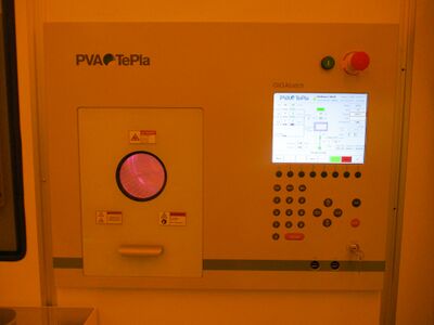
Plasma asher 4 in cleanroom E-5.

Product name: PVA Tepla Gigabatch 380M
Year of purchase: 2024

The Plasma Asher 4 can be used for the following processes:

  • Photoresist stripping
  • Descumming
  • Surface cleaning
  • Removal of organic passivation layers and masks


Plasma asher 4 has the following material restrictions:

  • No metals allowed
  • No metal oxides allowed
  • No III-V materials allowed

The user manual, risk assessment, and contact information can be found in LabManager - requires login

Typical stripping parameters
Tested with 1.5 µm AZ 5214E on 100 mm silicon substrate.

  • O2: 100 sccm
  • N2: 100 sccm
  • Pressure (DSC): 1.3 mbar
  • Power: 1000 W
  • Time (single wafer): 20-30 minutes
  • Time (full boat): 90 minutes


Process gas ratio for plasma asher 4 & 5

Ashing rate as function of gas mix ratio when processing a single 100 mm wafer and when processing a full boat with 25 wafers. The green area (~50% N2) covers the optimum range for both situations.

The ashing rate is related to the gas mix, usually expressed as percentage of nitrogen of the total amount of gas. Process development tests found that a gas mix of 50% nitrogen gives the highest ashing rate for both processing single substrates and when processing a full boat with 25 substrates.

Please note that the ashing rate for a full boat is approximately ten times slower, than the processing time for a single substrate.

Single substrate Full boat
Test results Highest ashing rate at 30-80% Nitrogen Highest ashing rate at 50-70% Nitrogen
Wafers 1 25
Wafer size 100 mm 100 mm
Boat position Center of chamber Center of chamber
Test wafer position Center of boat Center of boat
Total gas flow rate 500 sccm 200 sccm
Gas mix ratio Tested parameter Tested parameter
Chamber pressure 1.25 mbar 1.3 mbar
Power 1000 W 1000 W
Test processing time 2 minutes 10 minutes
Test average temperature 43°C 47°C


Process chamber pressure for plasma asher 4 & 5

Ashing rate as function of chamber pressure when processing a single substrate and when processing a full boat with 25 substrates. The green area covers the optimum range (~1.3 mbar) for both situations.

The ashing rate is related to the chamber pressure during processing. Process development tests found that 1.3 mbar gives the highest ashing rate for both processing single substrates and when processing a full boat with 25 substrates.

Please note that the ashing rate for a full boat is approximately ten times slower, than the processing time for a single substrate.

Single substrate Full boat
Test results Highest ashing rate at 1.3 mbar Highest ashing rate at 1.4 mbar
Wafers 1 25
Wafer size 100 mm 100 mm
Boat position Center of chamber Center of chamber
Test wafer position Center of boat Center of boat
Total gas flow rate 150 sccm 200 sccm
Gas mix ratio 30% N2 50% N2
Chamber pressure Tested parameter Tested parameter
Power 1000 W 1000 W
Test processing time 2 minutes 10 minutes
Test average temperature 43°C 55°C


Process gas flow rate for plasma asher 4 & 5

Ashing rate as function of total gas flow when processing a single substrate and when processing a full boat with 25 wafers. The green area covers the optimum range (~200 sccm) for both situations.

The ashing rate is related to the total gas flow rate during processing. Process development tests found that 200 sccm gives the highest ashing rate for both processing single substrates and when processing a full boat with 25 substrates. The experiments indicate that the gas flow rate has only a minor impact on the ashing rate.

Please note that the ashing rate for a full boat is approximately ten times slower, than the processing time for a single substrate.

Single substrate Full boat
Test results Highest ashing rate at 200 sccm Highest ashing rate at 200 sccm
Wafers 1 25
Wafer size 100 mm 100 mm
Boat position Center of chamber Center of chamber
Test wafer position Center of boat Center of boat
Total gas flow rate Tested parameter Tested parameter
Gas mix ratio 30% N2 30% N2
Chamber pressure 1.3 mbar 1.3 mbar
Power 1000 W 1000 W
Test processing time 2 minutes 10 minutes
Test average temperature 43°C 47°C


Process power for plasma asher 4 & 5

Ashing rate as function of microwave power.

The ashing rate is related to the power used during processing. Higher power increases ashing rate.

Single substrate
Test results Ashing rate follows Power
Wafers 1
Wafer size 100 mm
Boat position Center of chamber
Test wafer position Center of boat
Total gas flow rate 200 sccm
Gas mix ratio 30% N2
Chamber pressure 1.3 mbar
Power Tested parameter
Test processing time 2 minutes
Test average temperature 40°C


Process temperature for plasma asher 4 & 5

Ashing rate as function of temperature.

The ashing rate is related to the temperature during processing. Higher temperature increases ashing rate.

Single substrate
Test results Ashing rate follows temperature
Wafers 1
Wafer size 100 mm
Boat position Center of chamber
Test wafer position Center of boat
Total gas flow rate 200 sccm
Gas mix ratio 30% N2
Chamber pressure 1.3 mbar
Power 1000 W
Test processing time 2 minutes
Test average temperature Tested parameter


Comparison of ashing rate between substrate sizes for plasma asher 4 & 5

Comparison of ashing rate with different substrate sizes. Process was done using a single substrate placed in the middle of the glass boat, which was placed in the center of the chamber.

The ashing rate is highest for 100 mm substrates, lower for 150 mm substrates and even lower for 200 mm substrates.

All substrate sizes follows the same pattern:

  • Ashing rate increases with a higher percentage nitrogen in the gas mix
  • Ashing rate increases with a higher chamber pressure
  • The total gas flow has only little influence on the ashing rate, but slightly favors the lower flow rate of 200 sccm, similar to previous experiment results


Process parameter impact on ashing rate
Investigating the ashing rate using linear regression models on the process parameters, indicates that the gas mix and the chamber pressure has a significant impact on the ashing rate, while the gas flow has only little effect:


Plasma Asher 5

Plasma asher 5 in cleanroom E-5.

Product name: PVA Tepla Gigabatch 380M
Year of purchase: 2024

The Plasma Asher 5 can be used for the following processes:

  • Photoresist stripping
  • Descumming
  • Surface cleaning
  • Removal of organic passivation layers and masks


Furthermore plasma processing using CF4 in plasma asher 5 can be used for:

  • Etching of glass and ceramic
  • Etching of SiO2, Si3N4, Si
  • Removal of polyimide layers


Plasma asher 5 can be used for almost every material, but if you have any doubt if your materials are compatible/allowed in plasma asher 5, feel free to ask the lithography group at Nanolab.

The user manual, risk assessment, and contact information can be found in LabManager - requires login

Process Information

Plasma asher 5 is identical to plasma asher 4, see resist strip processing for plasma asher 4 here.


Processes specifically only for plasma asher 5:


Resist Strip
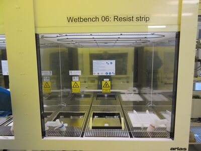
Resist strip bench in D-3

This resist strip is only for wafers without metal and SU-8.

There are one Remover 1165 bath for stripping and one IPA bath for rinsing.

Here are the main rules for resist strip use:

  • Place the wafers in a wafer holder and put them in the first bath for 10 min, this time is depending how much resist you have on the surface.
  • After the strip rinse your wafers in the IPA bath for 2-3 min.
  • Rinse your wafers for 4-5 min. in running water after stripping.


The user manual and contact information can be found in LabManager: Resist Strip - requires login


Overview of wet bench 06 and 07

Resist Strip Lift-off
Process Wet resist strip Metal lift-off process
Chemical Remover 1165 (NMP) Remover 1165 (NMP)
Process temperature Up to 65°C Up to 65°C
Substrate batch 1-25 wafers 1-25 wafers
Substrate size
  • 100 mm wafers
  • 150 mm wafers
  • 100 mm wafers
  • 150 mm wafers
Materials allowed
  • Silicon
  • Silicon oxide
  • Silicon nitride
  • Silicon oxynitride
All metals except Type IV (Pb, Te)