Specific Process Knowledge/Lithography/Strip: Difference between revisions
| (39 intermediate revisions by the same user not shown) | |||
| Line 18: | Line 18: | ||
! [[Specific Process Knowledge/Lithography/LiftOff|Lift-off]] | ! [[Specific Process Knowledge/Lithography/LiftOff|Lift-off]] | ||
|- | |- | ||
! scope=row| Purpose | ! scope=row style="text-align: left;" | Purpose | ||
| Resist descum | | Resist descum | ||
| | | | ||
| Line 29: | Line 29: | ||
| Metal lift-off | | Metal lift-off | ||
|- | |- | ||
! scope=row| Method | ! scope=row style="text-align: left;" | Method | ||
| Plasma ashing | | Plasma ashing | ||
| Plasma ashing | | Plasma ashing | ||
| Line 36: | Line 36: | ||
| Solvent & ultrasonication | | Solvent & ultrasonication | ||
|- | |- | ||
! scope=row| Process | ! scope=row style="text-align: left;" | Process gasses | ||
| O<sub>2</sub> (50 sccm) | | O<sub>2</sub> (50 sccm) | ||
| | | | ||
| Line 48: | Line 48: | ||
| NA | | NA | ||
|- | |- | ||
! scope=row| Process | ! scope=row style="text-align: left;" | Process power | ||
| 10-100 W (10-100%) | | 10-100 W (10-100%) | ||
| 150-1000 W | | 150-1000 W | ||
| Line 55: | Line 55: | ||
| NA | | NA | ||
|- | |- | ||
! scope=row| Process | ! scope=row style="text-align: left;" | Process solvent | ||
| NA | | NA | ||
| NA | | NA | ||
| Line 66: | Line 66: | ||
*IPA (rinsing agent) | *IPA (rinsing agent) | ||
|- | |- | ||
! scope=row| Substrate | ! scope=row style="text-align: left;" | Substrate batch | ||
| | | | ||
*Chips: several | *Chips: several | ||
| Line 90: | Line 90: | ||
*150 mm wafer: 1-25 | *150 mm wafer: 1-25 | ||
|- | |- | ||
! scope=row| Substrate | ! scope=row style="text-align: left;" | Substrate materials | ||
| | | | ||
*<span style="color:red">'''No polymer substrates'''</span><br> | *<span style="color:red">'''No polymer substrates'''</span><br> | ||
| Line 130: | Line 130: | ||
= Plasma Ashing process parameters= | = Plasma Ashing process parameters= | ||
{| | {| class="wikitable" | ||
|- | |- | ||
! !! [[Specific_Process_Knowledge/Lithography/Strip#Plasma_Asher_4|Resist stripping (PA4 & PA5)]] !! [[Specific_Process_Knowledge/Lithography/Descum#Plasma_Asher_3:_Descum|Descum (PA3)]] !! [[Specific_Process_Knowledge/Lithography/Descum#Plasma_Asher_4|Descum (PA4 & PA5)]] !! Surface treatment !! Other ashing of organic material | |||
| | |- | ||
| | ! scope=row style="text-align: left;" | Process pressure | ||
! | | 1.3 mbar || 0.8 mbar || 1.3 mbar || 0.5-1.5 mbar || 0.5-1.5 mbar | ||
! [[Specific_Process_Knowledge/Lithography/Descum|Descum | |||
! Surface treatment | |||
! | |||
|- | |||
|1.3 mbar | |||
|1.3 mbar | |||
|0.5-1.5 mbar | |||
|0.5-1.5 mbar | |||
|- | |- | ||
! scope=row style="text-align: left;" | Process gasses | |||
| | |||
| | |||
*O<sub>2</sub> (100 sccm) | *O<sub>2</sub> (100 sccm) | ||
*N<sub>2</sub> (100 sccm) | *N<sub>2</sub> (100 sccm) | ||
| | |||
*O<sub>2</sub> (45 sccm) | |||
| | | | ||
*O<sub>2</sub> (100 sccm) | *O<sub>2</sub> (100 sccm) | ||
*N<sub>2</sub> (100 sccm) | *N<sub>2</sub> (100 sccm) | ||
|O<sub>2</sub> | | | ||
|O<sub>2</sub> | *O<sub>2</sub> | ||
*N<sub>2</sub> | |||
*CF<sub>4</sub> | |||
| | |||
*O<sub>2</sub> | |||
|- | |- | ||
! scope=row style="text-align: left;" | Process power | |||
| 1000 W || 100 W || 200 W || 150-1000 W || 150-1000 W | |||
| | |||
| | |||
| | |||
| | |||
|- | |- | ||
! scope=row style="text-align: left;" | Process time | |||
| 20-90 minutes || 1-10 minutes || 5-15 minutes || Seconds to minutes || Many hours, material dependent | |||
|1- | |||
| | |||
| | |||
| | |||
|- | |- | ||
! scope=row style="text-align: left;" | Substrate batch | |||
| 1-25 || 1-2 || 1-25 || 1 || 1 | |||
|} | |} | ||
<br clear="all" /> | <br clear="all" /> | ||
=Plasma Asher 1= | =Plasma Asher 1= | ||
| Line 215: | Line 169: | ||
[[Specific Process Knowledge/Lithography/Strip/PlasmaAsher1|Information about decommissioned tool can be found here.]] | [[Specific Process Knowledge/Lithography/Strip/PlasmaAsher1|Information about decommissioned tool can be found here.]] | ||
<br clear="all" /> | |||
=Plasma Asher 2= | =Plasma Asher 2= | ||
| Line 220: | Line 175: | ||
[[Specific Process Knowledge/Lithography/Strip/PlasmaAsher2|Information about decommissioned tool can be found here.]] | [[Specific Process Knowledge/Lithography/Strip/PlasmaAsher2|Information about decommissioned tool can be found here.]] | ||
<br clear="all" /> | |||
=Plasma Asher 3: Descum= | =Plasma Asher 3: Descum= | ||
[[image:2017-03-15 13.12.45.jpg| | [[image:2017-03-15 13.12.45.jpg|400px|thumb|Plasma Asher 3: Descum is a low power plasma asher dedicated for descumming on smaller substrates.]] | ||
Product name: Diener Pico Plasma Asher<br> | Product name: Diener Pico Plasma Asher<br> | ||
Year of purchase: 2014 | Year of purchase: 2014 | ||
| Line 234: | Line 190: | ||
Pressure: 0.2-0.8 mbar<br> | Pressure: 0.2-0.8 mbar<br> | ||
Gas: 45 sccm O<sub>2</sub><br> | Gas: 45 sccm O<sub>2</sub><br> | ||
Power: 100%<br> | Power: 100 W (100%)<br> | ||
Time: 1 -10 minutes (depending on photoresist type and thickness)<br> | Time: 1 -10 minutes (depending on photoresist type and thickness)<br> | ||
| Line 245: | Line 201: | ||
<br clear="all" /> | <br clear="all" /> | ||
=Plasma Asher 4= | =Plasma Asher 4= | ||
[[File:PA5 front.jpg| | [[File:PA5 front.jpg|400px|thumb|Plasma asher 4 in cleanroom E-5.|right]] | ||
Product name: PVA Tepla Gigabatch 380M<br> | Product name: PVA Tepla Gigabatch 380M<br> | ||
Year of purchase: 2024 | Year of purchase: 2024 | ||
| Line 276: | Line 221: | ||
The user manual, risk assessment, and contact information can be found in [http://labmanager.dtu.dk/function.php?module=Machine&view=view&mach=530 LabManager] - '''requires login''' | The user manual, risk assessment, and contact information can be found in [http://labmanager.dtu.dk/function.php?module=Machine&view=view&mach=530 LabManager] - '''requires login''' | ||
'''Typical | '''Typical stripping parameters'''<br> | ||
Tested with 1.5 µm AZ 5214E on 100 mm silicon substrate. | |||
*O<sub>2</sub>: 100 sccm | *O<sub>2</sub>: 100 sccm | ||
*N<sub>2</sub>: 100 sccm | *N<sub>2</sub>: 100 sccm | ||
| Line 294: | Line 240: | ||
{| class="wikitable" | {| class="wikitable" | ||
|- | |- | ||
! | ! !! Single substrate !! Full boat | ||
|- | |- | ||
! scope=row| Test results | ! scope=row style="text-align: left;" | Test results | ||
| Highest ashing rate at 30-80% Nitrogen || Highest ashing rate at 50-70% Nitrogen | | Highest ashing rate at 30-80% Nitrogen || Highest ashing rate at 50-70% Nitrogen | ||
|- | |- | ||
! scope=row| Wafers | ! scope=row style="text-align: left;" | Wafers | ||
| 1 || 25 | | 1 || 25 | ||
|- | |- | ||
! scope=row| Wafer size | ! scope=row style="text-align: left;" | Wafer size | ||
| 100 mm || 100 mm | | 100 mm || 100 mm | ||
|- | |- | ||
! scope=row| Boat position | ! scope=row style="text-align: left;" | Boat position | ||
| Center of chamber || Center of chamber | | Center of chamber || Center of chamber | ||
|- | |- | ||
! scope=row| Test wafer position | ! scope=row style="text-align: left;" | Test wafer position | ||
| Center of boat || Center of boat | | Center of boat || Center of boat | ||
|- | |- | ||
! scope=row| Total gas flow rate | ! scope=row style="text-align: left;" | Total gas flow rate | ||
| 500 sccm || 200 sccm | | 500 sccm || 200 sccm | ||
|- | |- | ||
! scope=row| Gas mix ratio | ! scope=row style="text-align: left;" | Gas mix ratio | ||
| Tested parameter || Tested parameter | | Tested parameter || Tested parameter | ||
|- | |- | ||
! scope=row| Chamber pressure | ! scope=row style="text-align: left;" | Chamber pressure | ||
| 1.25 mbar || 1.3 mbar | | 1.25 mbar || 1.3 mbar | ||
|- | |- | ||
! scope=row| Power | ! scope=row style="text-align: left;" | Power | ||
| 1000 W || 1000 W | | 1000 W || 1000 W | ||
|- | |- | ||
! scope=row| Test processing time | ! scope=row style="text-align: left;" | Test processing time | ||
| 2 minutes || 10 minutes | | 2 minutes || 10 minutes | ||
|- | |- | ||
! scope=row| Test average temperature | ! scope=row style="text-align: left;" | Test average temperature | ||
| 43°C || 47°C | | 43°C || 47°C | ||
|} | |} | ||
| Line 340: | Line 286: | ||
{| class="wikitable" | {| class="wikitable" | ||
|- | |- | ||
! | ! !! Single substrate !! Full boat | ||
|- | |- | ||
! scope=row| Test results | ! scope=row style="text-align: left;" | Test results | ||
| Highest ashing rate at 1.3 mbar || Highest ashing rate at 1.4 mbar | | Highest ashing rate at 1.3 mbar || Highest ashing rate at 1.4 mbar | ||
|- | |- | ||
! scope=row| Wafers | ! scope=row style="text-align: left;" | Wafers | ||
| 1 || 25 | | 1 || 25 | ||
|- | |- | ||
! scope=row| Wafer size | ! scope=row style="text-align: left;" | Wafer size | ||
| 100 mm || 100 mm | | 100 mm || 100 mm | ||
|- | |- | ||
! scope=row| Boat position | ! scope=row style="text-align: left;" | Boat position | ||
| Center of chamber || Center of chamber | | Center of chamber || Center of chamber | ||
|- | |- | ||
! scope=row| Test wafer position | ! scope=row style="text-align: left;" | Test wafer position | ||
| Center of boat || Center of boat | | Center of boat || Center of boat | ||
|- | |- | ||
! scope=row| Total gas flow rate | ! scope=row style="text-align: left;" | Total gas flow rate | ||
| 150 sccm || 200 sccm | | 150 sccm || 200 sccm | ||
|- | |- | ||
! scope=row| Gas mix ratio | ! scope=row style="text-align: left;" | Gas mix ratio | ||
| 30% N<sub>2</sub> || 50% N<sub>2</sub> | | 30% N<sub>2</sub> || 50% N<sub>2</sub> | ||
|- | |- | ||
! scope=row| Chamber pressure | ! scope=row style="text-align: left;" | Chamber pressure | ||
| Tested parameter || Tested parameter | | Tested parameter || Tested parameter | ||
|- | |- | ||
! scope=row| Power | ! scope=row style="text-align: left;" | Power | ||
| 1000 W || 1000 W | | 1000 W || 1000 W | ||
|- | |- | ||
! scope=row| Test processing time | ! scope=row style="text-align: left;" | Test processing time | ||
| 2 minutes || 10 minutes | | 2 minutes || 10 minutes | ||
|- | |- | ||
! scope=row| Test average temperature | ! scope=row style="text-align: left;" | Test average temperature | ||
| 43°C || 55°C | | 43°C || 55°C | ||
|} | |} | ||
| Line 386: | Line 332: | ||
{| class="wikitable" | {| class="wikitable" | ||
|- | |- | ||
! | ! !! Single substrate !! Full boat | ||
|- | |- | ||
! scope=row| Test results | ! scope=row style="text-align: left;" | Test results | ||
| Highest ashing rate at 200 sccm || Highest ashing rate at 200 sccm | | Highest ashing rate at 200 sccm || Highest ashing rate at 200 sccm | ||
|- | |- | ||
! scope=row| Wafers | ! scope=row style="text-align: left;" | Wafers | ||
| 1 || 25 | | 1 || 25 | ||
|- | |- | ||
! scope=row| Wafer size | ! scope=row style="text-align: left;" | Wafer size | ||
| 100 mm || 100 mm | | 100 mm || 100 mm | ||
|- | |- | ||
! scope=row| Boat position | ! scope=row style="text-align: left;" | Boat position | ||
| Center of chamber || Center of chamber | | Center of chamber || Center of chamber | ||
|- | |- | ||
! scope=row| Test wafer position | ! scope=row style="text-align: left;" | Test wafer position | ||
| Center of boat || Center of boat | | Center of boat || Center of boat | ||
|- | |- | ||
! scope=row| Total gas flow rate | ! scope=row style="text-align: left;" | Total gas flow rate | ||
| Tested parameter || Tested parameter | | Tested parameter || Tested parameter | ||
|- | |- | ||
! scope=row| Gas mix ratio | ! scope=row style="text-align: left;" | Gas mix ratio | ||
| 30% N<sub>2</sub> || 30% N<sub>2</sub> | | 30% N<sub>2</sub> || 30% N<sub>2</sub> | ||
|- | |- | ||
! scope=row| Chamber pressure | ! scope=row style="text-align: left;" | Chamber pressure | ||
| 1.3 mbar || 1.3 mbar | | 1.3 mbar || 1.3 mbar | ||
|- | |- | ||
! scope=row| Power | ! scope=row style="text-align: left;" | Power | ||
| 1000 W || 1000 W | | 1000 W || 1000 W | ||
|- | |- | ||
! scope=row| Test processing time | ! scope=row style="text-align: left;" | Test processing time | ||
| 2 minutes || 10 minutes | | 2 minutes || 10 minutes | ||
|- | |- | ||
! scope=row| Test average temperature | ! scope=row style="text-align: left;" | Test average temperature | ||
| 43°C || 47°C | | 43°C || 47°C | ||
|} | |} | ||
| Line 430: | Line 376: | ||
{| class="wikitable" | {| class="wikitable" | ||
|- | |- | ||
! | ! !! Single substrate | ||
|- | |- | ||
! scope=row| Test results | ! scope=row style="text-align: left;" | Test results | ||
| Ashing rate follows | | Ashing rate follows Power | ||
|- | |- | ||
! scope=row| Wafers | ! scope=row style="text-align: left;" | Wafers | ||
| 1 | | 1 | ||
|- | |- | ||
! scope=row| Wafer size | ! scope=row style="text-align: left;" | Wafer size | ||
| 100 mm | | 100 mm | ||
|- | |- | ||
! scope=row| Boat position | ! scope=row style="text-align: left;" | Boat position | ||
| Center of chamber | | Center of chamber | ||
|- | |- | ||
! scope=row| Test wafer position | ! scope=row style="text-align: left;" | Test wafer position | ||
| Center of boat | | Center of boat | ||
|- | |- | ||
! scope=row| Total gas flow rate | ! scope=row style="text-align: left;" | Total gas flow rate | ||
| 200 sccm | | 200 sccm | ||
|- | |- | ||
! scope=row| Gas mix ratio | ! scope=row style="text-align: left;" | Gas mix ratio | ||
| 30% N<sub>2</sub> | | 30% N<sub>2</sub> | ||
|- | |- | ||
! scope=row| Chamber pressure | ! scope=row style="text-align: left;" | Chamber pressure | ||
| 1.3 mbar | | 1.3 mbar | ||
|- | |- | ||
! scope=row| Power | ! scope=row style="text-align: left;" | Power | ||
| | | Tested parameter | ||
|- | |- | ||
! scope=row| Test processing time | ! scope=row style="text-align: left;" | Test processing time | ||
| 2 minutes | | 2 minutes | ||
|- | |- | ||
! scope=row| Test average temperature | ! scope=row style="text-align: left;" | Test average temperature | ||
| | | 40°C | ||
|} | |} | ||
| Line 474: | Line 420: | ||
{| class="wikitable" | {| class="wikitable" | ||
|- | |- | ||
! | ! !! Single substrate | ||
|- | |- | ||
! scope=row| Test results | ! scope=row style="text-align: left;" | Test results | ||
| Ashing rate follows | | Ashing rate follows temperature | ||
|- | |- | ||
! scope=row| Wafers | ! scope=row style="text-align: left;" | Wafers | ||
| 1 | | 1 | ||
|- | |- | ||
! scope=row| Wafer size | ! scope=row style="text-align: left;" | Wafer size | ||
| 100 mm | | 100 mm | ||
|- | |- | ||
! scope=row| Boat position | ! scope=row style="text-align: left;" | Boat position | ||
| Center of chamber | | Center of chamber | ||
|- | |- | ||
! scope=row| Test wafer position | ! scope=row style="text-align: left;" | Test wafer position | ||
| Center of boat | | Center of boat | ||
|- | |- | ||
! scope=row| Total gas flow rate | ! scope=row style="text-align: left;" | Total gas flow rate | ||
| 200 sccm | | 200 sccm | ||
|- | |- | ||
! scope=row| Gas mix ratio | ! scope=row style="text-align: left;" | Gas mix ratio | ||
| 30% N<sub>2</sub> | | 30% N<sub>2</sub> | ||
|- | |- | ||
! scope=row| Chamber pressure | ! scope=row style="text-align: left;" | Chamber pressure | ||
| 1.3 mbar | | 1.3 mbar | ||
|- | |- | ||
! scope=row| Power | ! scope=row style="text-align: left;" | Power | ||
| | | 1000 W | ||
|- | |- | ||
! scope=row| Test processing time | ! scope=row style="text-align: left;" | Test processing time | ||
| 2 minutes | | 2 minutes | ||
|- | |- | ||
! scope=row| Test average temperature | ! scope=row style="text-align: left;" | Test average temperature | ||
| | | Tested parameter | ||
|} | |} | ||
| Line 534: | Line 480: | ||
=Plasma Asher 5= | =Plasma Asher 5= | ||
[[File:PA5 front.jpg| | [[File:PA5 front.jpg|400px|thumb|Plasma asher 5 in cleanroom E-5.|right]] | ||
Product name: PVA Tepla Gigabatch 380M<br> | Product name: PVA Tepla Gigabatch 380M<br> | ||
Year of purchase: 2024 | Year of purchase: 2024 | ||
| Line 549: | Line 495: | ||
*Etching of SiO<sub>2</sub>, Si<sub>3</sub>N<sub>4</sub>, Si | *Etching of SiO<sub>2</sub>, Si<sub>3</sub>N<sub>4</sub>, Si | ||
*Removal of polyimide layers | *Removal of polyimide layers | ||
| Line 567: | Line 502: | ||
===Process Information=== | ===Process Information=== | ||
Plasma asher 5 is identical to plasma asher 4, see resist strip processing for plasma asher 4 [[Specific_Process_Knowledge/Lithography/Strip# | Plasma asher 5 is identical to plasma asher 4, see resist strip processing for plasma asher 4 [[Specific_Process_Knowledge/Lithography/Strip#Plasma_Asher_4|here]]. | ||
''' | '''Processes specifically only for plasma asher 5:'''<br> | ||
*[[Specific Process Knowledge/Etch/Etching of Silicon Oxide/SiO2 etch using Plasma Asher |SiO<sub>2</sub> etch using Plasma Asher 1]] | *[[Specific Process Knowledge/Etch/Etching of Silicon Oxide/SiO2 etch using Plasma Asher |SiO<sub>2</sub> etch using Plasma Asher 1]] | ||
*[[Specific Process Knowledge/Lithography/Descum#Plasma Asher 5|Descum using plasma asher 5]] | *[[Specific Process Knowledge/Lithography/Descum#Plasma Asher 5|Descum using plasma asher 5]] | ||
| Line 576: | Line 512: | ||
=Resist Strip= | =Resist Strip= | ||
[[Image:Resist_strip.jpg| | [[Image:Resist_strip.jpg|400px|thumb|Resist strip bench in D-3]] | ||
This resist strip is only for wafers without metal and SU-8. | This resist strip is only for wafers without metal and SU-8. | ||
| Line 593: | Line 529: | ||
==Overview of wet bench 06 and 07== | ==Overview of wet bench 06 and 07== | ||
{| class="wikitable" | |||
{| | |- | ||
! !! [[Specific Process Knowledge/Lithography/Strip#Resist_Strip|Resist Strip]] !! [[Specific Process Knowledge/Lithography/LiftOff#Lift-off_wet_bench_07|Lift-off]] | |||
|- | |- | ||
! scope=row style="text-align: left;" | Process | |||
! [[Specific Process Knowledge/Lithography/Strip#Resist_Strip|Resist Strip]] | | Wet resist strip || Metal lift-off process | ||
! [[Specific Process Knowledge/Lithography/LiftOff#Lift-off_wet_bench_07|Lift-off]] | |||
|- | |||
|Wet | |||
| | |||
|- | |- | ||
! scope=row style="text-align: left;" | Chemical | |||
| Remover 1165 (NMP) || Remover 1165 (NMP) | |||
| | |||
| | |||
|- | |- | ||
! scope=row style="text-align: left;" | Process temperature | |||
| Up to 65°C || Up to 65°C | |||
|Up to 65°C | |||
|Up to 65°C | |||
|- | |- | ||
! scope=row style="text-align: left;" | Substrate batch | |||
| 1-25 wafers || 1-25 wafers | |||
| | |||
1 - 25 wafers | |||
| | |||
1 - 25 wafers | |||
|- | |- | ||
! scope=row style="text-align: left;" | Substrate size | |||
| | |||
| | |||
*100 mm wafers | *100 mm wafers | ||
*150 mm wafers | *150 mm wafers | ||
| Line 637: | Line 553: | ||
*150 mm wafers | *150 mm wafers | ||
|- | |- | ||
! scope=row style="text-align: left;" | Materials allowed | |||
| | |||
| | |||
*Silicon | *Silicon | ||
*Silicon | *Silicon oxide | ||
*Silicon | *Silicon nitride | ||
*Silicon | *Silicon oxynitride | ||
| | | All metals except Type IV (Pb, Te) | ||
All metals except Type IV (Pb, Te) | |||
|} | |} | ||
<br clear="all" /> | |||
Latest revision as of 11:34, 29 September 2025
The content on this page, including all images and pictures, was created by DTU Nanolab staff, unless otherwise stated.
Feedback to this page: click here
Strip Comparison Table
| Plasma Asher 3: Descum | Plasma Asher 4 (Clean) | Plasma Asher 5 (Dirty) | Resist strip | Lift-off | |
|---|---|---|---|---|---|
| Purpose | Resist descum |
|
|
Resist stripping | Metal lift-off |
| Method | Plasma ashing | Plasma ashing | Plasma ashing | Solvent & ultrasonication | Solvent & ultrasonication |
| Process gasses | O2 (50 sccm) |
|
|
NA | NA |
| Process power | 10-100 W (10-100%) | 150-1000 W | 150-1000 W | NA | NA |
| Process solvent | NA | NA | NA |
|
|
| Substrate batch |
|
|
|
|
|
| Substrate materials |
|
|
|
|
|
Plasma Ashing process parameters
| Resist stripping (PA4 & PA5) | Descum (PA3) | Descum (PA4 & PA5) | Surface treatment | Other ashing of organic material | |
|---|---|---|---|---|---|
| Process pressure | 1.3 mbar | 0.8 mbar | 1.3 mbar | 0.5-1.5 mbar | 0.5-1.5 mbar |
| Process gasses |
|
|
|
|
|
| Process power | 1000 W | 100 W | 200 W | 150-1000 W | 150-1000 W |
| Process time | 20-90 minutes | 1-10 minutes | 5-15 minutes | Seconds to minutes | Many hours, material dependent |
| Substrate batch | 1-25 | 1-2 | 1-25 | 1 | 1 |
Plasma Asher 1
Plasma asher 1 was decommissioned 2024-12-02.
Information about decommissioned tool can be found here.
Plasma Asher 2
Plasma asher 2 was decommissioned 2024-12-02.
Information about decommissioned tool can be found here.
Plasma Asher 3: Descum

Product name: Diener Pico Plasma Asher
Year of purchase: 2014
The Plasma Asher 3: Descum is dedicated for resist descum, i.e. removal of remains resist traces after development. It has a small chamber, so you can only load a single 100 mm substrate, or a few smaller pieces.
In this machine, only Oxygen is used for processing.
Typical process parameters:
Process: Photoresist descumming
Pressure: 0.2-0.8 mbar
Gas: 45 sccm O2
Power: 100 W (100%)
Time: 1 -10 minutes (depending on photoresist type and thickness)
Other materials have not been tested.
The user manual, user APV, and contact information can be found in LabManager - requires login
Process Information
Detailed information about descum processing on Plasma asher 3: Descum can be found here.
Plasma Asher 4

Product name: PVA Tepla Gigabatch 380M
Year of purchase: 2024
The Plasma Asher 4 can be used for the following processes:
- Photoresist stripping
- Descumming
- Surface cleaning
- Removal of organic passivation layers and masks
Plasma asher 4 has the following material restrictions:
- No metals allowed
- No metal oxides allowed
- No III-V materials allowed
The user manual, risk assessment, and contact information can be found in LabManager - requires login
Typical stripping parameters
Tested with 1.5 µm AZ 5214E on 100 mm silicon substrate.
- O2: 100 sccm
- N2: 100 sccm
- Pressure (DSC): 1.3 mbar
- Power: 1000 W
- Time (single wafer): 20-30 minutes
- Time (full boat): 90 minutes
Process gas ratio for plasma asher 4 & 5

The ashing rate is related to the gas mix, usually expressed as percentage of nitrogen of the total amount of gas. Process development tests found that a gas mix of 50% nitrogen gives the highest ashing rate for both processing single substrates and when processing a full boat with 25 substrates.
Please note that the ashing rate for a full boat is approximately ten times slower, than the processing time for a single substrate.
| Single substrate | Full boat | |
|---|---|---|
| Test results | Highest ashing rate at 30-80% Nitrogen | Highest ashing rate at 50-70% Nitrogen |
| Wafers | 1 | 25 |
| Wafer size | 100 mm | 100 mm |
| Boat position | Center of chamber | Center of chamber |
| Test wafer position | Center of boat | Center of boat |
| Total gas flow rate | 500 sccm | 200 sccm |
| Gas mix ratio | Tested parameter | Tested parameter |
| Chamber pressure | 1.25 mbar | 1.3 mbar |
| Power | 1000 W | 1000 W |
| Test processing time | 2 minutes | 10 minutes |
| Test average temperature | 43°C | 47°C |
Process chamber pressure for plasma asher 4 & 5

The ashing rate is related to the chamber pressure during processing. Process development tests found that 1.3 mbar gives the highest ashing rate for both processing single substrates and when processing a full boat with 25 substrates.
Please note that the ashing rate for a full boat is approximately ten times slower, than the processing time for a single substrate.
| Single substrate | Full boat | |
|---|---|---|
| Test results | Highest ashing rate at 1.3 mbar | Highest ashing rate at 1.4 mbar |
| Wafers | 1 | 25 |
| Wafer size | 100 mm | 100 mm |
| Boat position | Center of chamber | Center of chamber |
| Test wafer position | Center of boat | Center of boat |
| Total gas flow rate | 150 sccm | 200 sccm |
| Gas mix ratio | 30% N2 | 50% N2 |
| Chamber pressure | Tested parameter | Tested parameter |
| Power | 1000 W | 1000 W |
| Test processing time | 2 minutes | 10 minutes |
| Test average temperature | 43°C | 55°C |
Process gas flow rate for plasma asher 4 & 5

The ashing rate is related to the total gas flow rate during processing. Process development tests found that 200 sccm gives the highest ashing rate for both processing single substrates and when processing a full boat with 25 substrates. The experiments indicate that the gas flow rate has only a minor impact on the ashing rate.
Please note that the ashing rate for a full boat is approximately ten times slower, than the processing time for a single substrate.
| Single substrate | Full boat | |
|---|---|---|
| Test results | Highest ashing rate at 200 sccm | Highest ashing rate at 200 sccm |
| Wafers | 1 | 25 |
| Wafer size | 100 mm | 100 mm |
| Boat position | Center of chamber | Center of chamber |
| Test wafer position | Center of boat | Center of boat |
| Total gas flow rate | Tested parameter | Tested parameter |
| Gas mix ratio | 30% N2 | 30% N2 |
| Chamber pressure | 1.3 mbar | 1.3 mbar |
| Power | 1000 W | 1000 W |
| Test processing time | 2 minutes | 10 minutes |
| Test average temperature | 43°C | 47°C |
Process power for plasma asher 4 & 5

The ashing rate is related to the power used during processing. Higher power increases ashing rate.
| Single substrate | |
|---|---|
| Test results | Ashing rate follows Power |
| Wafers | 1 |
| Wafer size | 100 mm |
| Boat position | Center of chamber |
| Test wafer position | Center of boat |
| Total gas flow rate | 200 sccm |
| Gas mix ratio | 30% N2 |
| Chamber pressure | 1.3 mbar |
| Power | Tested parameter |
| Test processing time | 2 minutes |
| Test average temperature | 40°C |
Process temperature for plasma asher 4 & 5

The ashing rate is related to the temperature during processing. Higher temperature increases ashing rate.
| Single substrate | |
|---|---|
| Test results | Ashing rate follows temperature |
| Wafers | 1 |
| Wafer size | 100 mm |
| Boat position | Center of chamber |
| Test wafer position | Center of boat |
| Total gas flow rate | 200 sccm |
| Gas mix ratio | 30% N2 |
| Chamber pressure | 1.3 mbar |
| Power | 1000 W |
| Test processing time | 2 minutes |
| Test average temperature | Tested parameter |
Comparison of ashing rate between substrate sizes for plasma asher 4 & 5

The ashing rate is highest for 100 mm substrates, lower for 150 mm substrates and even lower for 200 mm substrates.
All substrate sizes follows the same pattern:
- Ashing rate increases with a higher percentage nitrogen in the gas mix
- Ashing rate increases with a higher chamber pressure
- The total gas flow has only little influence on the ashing rate, but slightly favors the lower flow rate of 200 sccm, similar to previous experiment results
Process parameter impact on ashing rate
Investigating the ashing rate using linear regression models on the process parameters, indicates that the gas mix and the chamber pressure has a significant impact on the ashing rate, while the gas flow has only little effect:
-
 100 mm parameter impact
 -
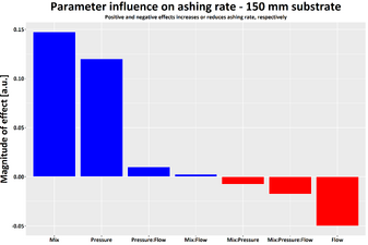 150 mm parameter impact
 -
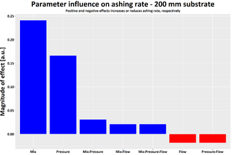 200 mm parameter impact


Plasma Asher 5
Product name: PVA Tepla Gigabatch 380M
Year of purchase: 2024
The Plasma Asher 5 can be used for the following processes:
- Photoresist stripping
- Descumming
- Surface cleaning
- Removal of organic passivation layers and masks
Furthermore plasma processing using CF4 in plasma asher 5 can be used for:
- Etching of glass and ceramic
- Etching of SiO2, Si3N4, Si
- Removal of polyimide layers
Plasma asher 5 can be used for almost every material, but if you have any doubt if your materials are compatible/allowed in plasma asher 5, feel free to ask the lithography group at Nanolab.
The user manual, risk assessment, and contact information can be found in LabManager - requires login
Process Information
Plasma asher 5 is identical to plasma asher 4, see resist strip processing for plasma asher 4 here.
Processes specifically only for plasma asher 5:
Resist Strip

This resist strip is only for wafers without metal and SU-8.
There are one Remover 1165 bath for stripping and one IPA bath for rinsing.
Here are the main rules for resist strip use:
- Place the wafers in a wafer holder and put them in the first bath for 10 min, this time is depending how much resist you have on the surface.
- After the strip rinse your wafers in the IPA bath for 2-3 min.
- Rinse your wafers for 4-5 min. in running water after stripping.
The user manual and contact information can be found in LabManager: Resist Strip - requires login
Overview of wet bench 06 and 07
| Resist Strip | Lift-off | |
|---|---|---|
| Process | Wet resist strip | Metal lift-off process |
| Chemical | Remover 1165 (NMP) | Remover 1165 (NMP) |
| Process temperature | Up to 65°C | Up to 65°C |
| Substrate batch | 1-25 wafers | 1-25 wafers |
| Substrate size |
|
|
| Materials allowed |
|
All metals except Type IV (Pb, Te) |