LabAdviser/Process Flow/Solar cell process flow: Difference between revisions
| (4 intermediate revisions by the same user not shown) | |||
| Line 25: | Line 25: | ||
<br clear="all" />A detailed process flow for the solar cell process flow, including all steps and process parameters, can be found here: | <br clear="all" />A detailed process flow for the solar cell process flow, including all steps and process parameters, can be found here: | ||
Process flow for the solar cell fabrication process as [[ | Process flow for the solar cell fabrication process as [[Media:Solar Cell process flow 2024.docx| Word-]] or [[Media:Solar Cell process flow 2024.pdf|PDF-File]]. | ||
==Process flow for a Simple Solar Cell== | ==Process flow for a Simple Solar Cell== | ||
| Line 117: | Line 117: | ||
|Expose photoresist in aligner | |Expose photoresist in aligner | ||
|The resist layer on the wafer frontside is exposed in the aligner, with a dark field mask. Align the mask to wafer flat, and use hard contact. | |The resist layer on the wafer frontside is exposed in the aligner, with a dark field mask. Align the mask to wafer flat, and use hard contact. | ||
|Here you can see a comparison between different [[ | |Here you can see a comparison between different [[Specific Process Knowledge/Lithography/UVExposure|aligners]]. | ||
|[[image:2 lithography mask 1.jpg|250x350px|center]] | |[[image:2 lithography mask 1.jpg|250x350px|center]] | ||
|- | |- | ||
| Line 278: | Line 278: | ||
|Expose photoresist in aligner | |Expose photoresist in aligner | ||
|The wafer needs to be aligned to the mask. "Hard contact" is recommended. | |The wafer needs to be aligned to the mask. "Hard contact" is recommended. | ||
|Here you can get information about exposure doses and development times depending on different resist types, thicknesses and equipment used. [[ | |Here you can get information about exposure doses and development times depending on different resist types, thicknesses and equipment used. [[Specific Process Knowledge/Lithography/Resist#Exposure dose|Lists of exposure doses and development times.]] | ||
|[[image:5 lithography mask 2.jpg|250x350px|center]] | |[[image:5 lithography mask 2.jpg|250x350px|center]] | ||
|- | |- | ||
| Line 286: | Line 286: | ||
|Develop photoresist | |Develop photoresist | ||
|In the development step the '''exposed resist is removed,''' and a resist pattern is formed on the surface. | |In the development step the '''exposed resist is removed,''' and a resist pattern is formed on the surface. | ||
|Comparison of different [[Specific Process Knowledge/Lithography/Development|developers]]. More details on development times dependent on equipment, resist, thickness and exposure doses can be seen here:[[ | |Comparison of different [[Specific Process Knowledge/Lithography/Development|developers]]. More details on development times dependent on equipment, resist, thickness and exposure doses can be seen here:[[Specific Process Knowledge/Lithography/Resist#Exposure dose|Lists of exposure doses and development times.]] | ||
|[[image:5_4_development.JPG|250x350px|center]] | |[[image:5_4_development.JPG|250x350px|center]] | ||
|- | |- | ||
| Line 470: | Line 470: | ||
|Stylus profiler inspection | |Stylus profiler inspection | ||
|Check the final result by measuring the profile of the aluminium structures on the wafer frontside with a stylus profilometer. | |Check the final result by measuring the profile of the aluminium structures on the wafer frontside with a stylus profilometer. | ||
|[[Specific Process Knowledge/Characterization/ | |[[Specific Process Knowledge/Characterization/Topographic measurement|Stylus profilers]] | ||
|[[image: Profile_After_lift_off_solar cell.JPG|250x350px|center]] | |[[image: Profile_After_lift_off_solar cell.JPG|250x350px|center]] | ||
|- | |- | ||
| Line 478: | Line 478: | ||
|4 point probe inspection | |4 point probe inspection | ||
|Measure the metal sheet resistance on the wafer backside with a 4 point probe. | |Measure the metal sheet resistance on the wafer backside with a 4 point probe. | ||
|[[ | |[[Specific Process Knowledge/Characterization/Four-Point Probe|4 point probe]] | ||
| | | | ||
|- | |- | ||
Latest revision as of 14:26, 17 June 2025
Feedback to this page: click here
Introduction
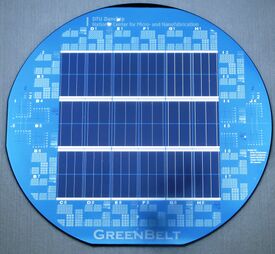
A solar cell (photovoltaic cell) converts light energy into electricity. When shining light on to the solar cell, photons will be absorbed by the p-doped silicon (absorber) and electron-hole pairs are generated in the crystal. Simultaneously, electron-hole pairs are generated near the p-n junction which contribute to a current flowing from the p- to the n-doped region. Negatively charged carriers move towards the n-doped region, while positively charged carriers move away from the n-doped region.
In order to use the generated electricity, the cell has to be placed in an electric circuit such that electrons can flow freely and continuously from the n-doped region to the p doped region through a load, e.g. a light bulb. To ease the flow of electrons metal contacts are made on each side of the cell. When the electrons reach the p-doped region through the backside contact they will recombine with the holes. An anti-reflective coating can be deposited on the front side of the solar cell to minimize the reflectance of the incoming light on the surface, and thereby harvesting more energy from the light source.
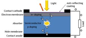
If we take a look at the cross-section of a simple silicon-based solar cell (figure 1), we see a structure as shown in figure 2. The solar cell consists of an absorber (p-doped bulk silicon crystal), an electron membrane (shallow n-doped layer on top of the silicon crystal) and metal contacts.
Fabrication of a Solar Cell
The fabrication of any device in the cleanroom starts with developing a process flow (recipe). The process flow includes all steps of the fabrication process in the right order, including crucial investigation methods to ensure quality control.
As a general rule of processing, all high temperature processes are done as early as possible, followed by low temperature processes and metal deposition. Since oxide growth and doping by diffusion are high temperature processes, we start by making the n-doped layer and anti-reflecting coating layer. This is done by growing a silicon oxide film and subsequently defining the areas that must be opened to allow doping with phosphorous. The pattering is done by UV lithography of a photo resist, followed by wet etching of the silicon oxide in opened areas and finally the removal of remaining resist. That leaves areas in the silicon open which can are then doped in a high temperature furnace with phosphorous. In a last high temperature furnace, the anti-reflecting coating is made by growing an oxide of a specific thickness (example process: 130 nm).
To make the metal contacts, we have to define the areas where contact to the n-doped layer on the front side is needed. This is done by opening the silicon oxide layer using another UV lithography step followed by another oxide wet etch. This etch step removes the oxide on the backside as well.
Finally, a last lithography step is carried out to define the shape of the contacts and interconnections on the front side. This is done by using a negative photoresist that allows for a metal lift-off process. Metal is evaporated on the defined resist pattern on the frontside as well as forming the contact anode on the backside. The resist is subsequently removed (lifted) in acetone or remover 1165 together with the excess metal only leaving metal at the defined areas and at the backside. This process is called lift-off.

A detailed process flow for the solar cell process flow, including all steps and process parameters, can be found here:
Process flow for the solar cell fabrication process as Word- or PDF-File.
Process flow for a Simple Solar Cell
Beneath you can see an example of a process recipe with all process steps needed to fabricate a wafer with solar cells. In the process you will find links to the actual machines and processes described in LabAdviser, where you can get more detailed information. Before doing the processing you also have to find the right processing parameters, they are not listed here.
Please note that some of the tools mayb not be up to date in the list below. However, the word and pdf file above have been updated in May 2024.
This is a sketchy description of how a solar cell can be fabricated (some details are omitted).
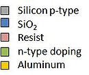
1 Thermal oxidation
| Step | Description | LabAdviser link | Image showing the step | |
|---|---|---|---|---|
| 1.1 | Si wafer | Start with a 100 mm Si<100> wafer that is single side polished and p doped with boron. This will be the absorber in the final solar cell. | Wafer information, types of avaliable wafers are listed. | |
| 1.2 | RCA clean | The wafer has to be RCA cleaned, before entering an oxidation furnace. | RCA cleaning, the different steps in the cleaning procedure are described. | |
| 1.3 | SiO2 dry oxidation | Grow a dry thermal oxide layer in the Boron Drive-in furnace (A1). The oxide layer will be patterned later on to define n-doped areas ("electron membrane".) | Boron Drive-in furnace, info about performance and process parameter range. |  |
2 Lithography and oxide etch
| Step | Description | LabAdviser link | Image showing the step | |
|---|---|---|---|---|
| 2.1 | HMDS surface treatment | To ensure the resist sticks to the surface, the wafer is HMDS treated before resist spinning. | HMDS oven | |
| 2.2 | Spin resist on wafer backside | The backside of the wafer needs to be protected, to prevent the SiO2 from being etched in the first etch step (section 3). | Information about which resist spinners can be used, and which types of resists are available. |  |
| 2.3 | Spin resist on wafer frontside | The frontside of the wafer is covered with a resist layer. | Information about resist processing. Process flows for positive, negative and reversed lithography processes. |  |
| 2.4 | Expose photoresist in aligner | The resist layer on the wafer frontside is exposed in the aligner, with a dark field mask. Align the mask to wafer flat, and use hard contact. | Here you can see a comparison between different aligners. | 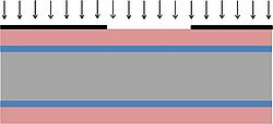 |
| 2.5 | Develop photoresist | In the development step the exposed resist is removed, so that a resist pattern is formed on the surface. | Comparison of different developers. |  |
| 2.6 | Optical microscope inspection | Check the results of the exposure and development with an optical microscope by inspecting that the pattern and alignment marks are clearly visible. Right image: top view of alignment marks. The alignment marks will be used to align the wafer to the mask in next lithography step (section 5). | The different optical microscopes and their features are listed. |  |
3 SiO2 etch
| Step | Description | LabAdviser link | Image showing the step | |
|---|---|---|---|---|
| 3.1 | SiO2 etch | Etch through the SiO2 layer, where the resist is not covering the SiO2, using Sioetch. Sioetch is BHF with a surfactant. | Wet silicon oxide etch (BHF). Etch rates for BHF and HF etches are listed for oxides deposited with different methods. |  |
| 3.2 | Inspection | Inspect the pattern and alignment marks with an optical microscope to check the result of the SiO2 etch. | The different optical microscopes and their features are listed. | |
| 3.3 | Strip resist | The resist is removed with acetone. First 2-3 min in rough followed by 5 min in fine strip bath with ultrasound. | Strip of resist in acetone with ultrasound. Rough and fine strip baths. |  |
4 Phosphorous doping
| Step | Description | LabAdviser link | Image showing the step | |
|---|---|---|---|---|
| 4.1 | RCA cleaning | The wafer has to be RCA cleaned, before entering a pre-deposition furnace. Skip the HF dip to prevent that some of the oxide is removed. | RCA cleaning, the different steps in the cleaning procedure are described. | |
| 4.2 | Phosphorus pre-deposition | Areas that should be n-doped have been defined by photolithography and etched, and in this step these areas are doped by diffusion in the Phosphorus Pre-dep furnace. | Phosphorus Pre-dep furnace (POCL). Here information about process temperatures and gasses are found. |  |
| 4.3 | Etch of phosphorus glass | All phosphorus glass and only some of the dry oxide is removed in this step by a BHF etch in the RCA bench for doped wafers. | BHF etch. | |
| 4.4 | SiO2 dry oxidation | An anti reflective coating is made by an oxide growth (of a specific thickness). | Phosphorous Drive-in furnace with information about performance and allowed substrates. |  |
5 Lithography – 1.5µm standard
| Step | Description | LabAdviser link | Image showing the step | |
|---|---|---|---|---|
| 5.1 | HMDS surface treatment | To ensure the resist sticks to the surface, the wafer is HMDS treated before resist spinning. | Different methods of pretreatment prior resist spinning. | |
| 5.2 | Spin resist on wafer frontside | The frontside of the wafer is covered with a resist layer | Information about which resist coaters can be used and technical reports for the different resist types. |  |
| 5.3 | Expose photoresist in aligner | The wafer needs to be aligned to the mask. "Hard contact" is recommended. | Here you can get information about exposure doses and development times depending on different resist types, thicknesses and equipment used. Lists of exposure doses and development times. |  |
| 5.4 | Develop photoresist | In the development step the exposed resist is removed, and a resist pattern is formed on the surface. | Comparison of different developers. More details on development times dependent on equipment, resist, thickness and exposure doses can be seen here:Lists of exposure doses and development times. |  |
| 5.5 | Optical microscope inspection | Check the pattern and alignment marks with an optical microscope. The alignment marks should be aligned to the marks from the previous lithography step (section 2). Right image: top view of alignment marks after second lithography step. | The different optical microscopes and their features are listed. |  |
6 SiO2 etch
| Step | Description | LabAdviser link | Image showing the step | |
|---|---|---|---|---|
| 6.1 | SiO2 etch | Remove oxide with Sioetch in the areas where the metallic contact (cathodes) will be placed (section 8). Sioetch is BHF with a surfactant. | Wet Silicon Oxide Etch (BHF). Etch rates for BHF and HF etches are listed for oxides deposited with different methods. |  |
| 6.2 | Optical microscope inspection | Inspect the pattern and alignment marks with an optical microscopes to check the result of the lithography step. The alignment marks should be clearly visible. | The different optical microscopes and their features are listed. | |
| 6.3 | Strip resist | The resist is removed with acetone. First 2-3 min in rough followed by 5 min in fine strip bath with ultrasound. | Comparison of different methods for removing resist. |  |
| 6.4 | Stylus profiler inspection | The step height of the SiO2 in the doped and undoped areas are measured after the SiO2 etch. | Stylus profilers. The different stylus profilers and their features are described. | |
7 Lithography - Negative process
| Step | Description | LabAdviser link | Image showing the step | |
|---|---|---|---|---|
| 7.1 | HMDS surface treatment | To ensure the resist sticks to the surface, the wafer is HMDS treated before resist spinning. | Several resist coaters can do the HMDS pretreatment. | |
| 7.2 | Spin resist on wafer frontside | The frontside of the wafer is covered with a resist layer. | Information about which resist coaters can be used, and which types of resists are available. The negative resist n-LOF 2020 are available in the automatic coater Spin Coater: Gamma UV and the manual coaters. |  |
| 7.3 | Expose resist in aligner | The resist is exposed in an aligner, with a bright field mask. The alignment marks on the wafer need to be aligned to the marks on the mask. "Hard contact" is recommended. | Details on alignment marks (if you would design a mask). |  |
| 7.4 | Post exposure bake (PEB) | For negative resist a PEB is crucial, where the wafer with resist is heated after exposure. | PEB can be done in the Developer TMAH UV-lithography, or on one of the hot plates and ovens. |  |
| 7.5 | Develop photoresist | The non-exposed resist is removed, so that a resist pattern is formed on the surface. The resist has negative sloped side walls due to the nature of a negative resist, which is good for lift-off. | Information about n-LOF2020 and the lift-off process. |  |
| 7.6 | Optical microscope inspection | Check the pattern and alignment marks with an optical microscope. The alignment marks should be aligned to the marks from the two previous lithography steps (section 2 and 5). Right image: alignment marks after the third lithography step. | The different optical microscopes and their features are listed. |  |
8 Aluminium pattern
| Step | Description | LabAdviser link | Image showing the step | |
|---|---|---|---|---|
| 8.1 | Aluminium deposition on wafer frontside | Deposit metal on the wafer frontside to fabricate contacts (contact cathodes). | Temescal: materials can be deposited in this tool. |  |
| 8.2 | Aluminium deposition on wafer backside | Deposit metal for contacts (contact anode) on the wafer backside. | Deposition of Aluminum can be done with several machines in the cleanroom. |  |
| 8.3 | Lift-off | Remove the resist and the metal deposited on top of the areas covered by resist. | Information about the lift-off process can be seen here. |  |
| 8.4 | Optical microscope inspection | Check the final result with an optical microscope. | Optical microscopes | |
| 8.5 | Stylus profiler inspection | Check the final result by measuring the profile of the aluminium structures on the wafer frontside with a stylus profilometer. | Stylus profilers | 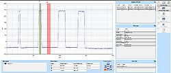 |
| 8.6 | 4 point probe inspection | Measure the metal sheet resistance on the wafer backside with a 4 point probe. | 4 point probe | |

