Specific Process Knowledge/Thin film deposition/Deposition of Silicon Oxide/Deposition of Silicon Oxide using PECVD
Feedback to this page: click here
This page is written by Berit Herstrøm @ DTU Nanolab (BGHE) if nothing else is stated
At the moment DTU Nanolab has 2 PECVDs that can deposit silicon oxide with or without dopants of boron, phosphorus. PECVD1 and PECVD2 has been decommissioned and now we have PECVD3 and PECVD4. PECVD3 are for silicon based processing allowing wafers with small amount of metal (<5% wafer coverage). PECVD4 is for clean wafers both for silicon based materials and for III-V materials. Look at the PECVD page to learn more about the PECVDs at Nanolab. All though PECVD4 and PECVD3 are very much alike you cannot count on that a recipe on one system will give exactly the same results on the other system.
Deposition of SiO2 with PECVD4
| Quality Control (QC) for PECVD4 - oxide | ||||||||||||||||||||||
|
| Recipe | Dep. rate [nm/min] | RI | Unif. [%] | Stress [MPa] | Comments | SiH4 [sccm] | N2O [sccm] | N2 [sccm] | B2H6 | PH3 | Pressure [mTorr] | Power [W] | Load | Tune | Time [mm:ss] | Tested
|
|---|---|---|---|---|---|---|---|---|---|---|---|---|---|---|---|---|
| LF SiO | 75-78 nm/min | 1.480-1.483 | ± 2.1-2.7% | compressive 309 MPa | Click for more results | 12 | 1420 | 392 | 550 mTorr | 60LF" | 1:15/13:00(stress) | February 2017 bghe | ||||
| HF SiO | 63-64 nm/min | 1.476-1.477 | ± 0.3-0.5% | Compressive: 250.5 MPa | Click for more results | 10 | 1420 | 392 | 900 mTorr | 30HF | 2:00/16:00(stress) | February 2017 bghe | ||||
| waveguide | 159.5 nm/min | 1.462 | ± 0.8% | Compressive: 121.9 MPa | 17 | 2000 | 300 mTorr | 700 LF | 40:00 | February 2017 bghe | ||||||
| BPSG | 259 nm/min | 1.4593 | ± 1.7% | Compressive: 36.7 MPa | Measured after anneal in Clad1000 | 17 | 1600 | 135 | 40 | 900 mTorr | 800 LF | 10:00/56:00(stress) | February 2017 bghe | |||
| BPSG low stress | 302 nm/min | 1.4598 | ± 1.7% | Compressive: 1.4 MPa | Measured after anneal in Clad1000 | 17 | 1600 | 240 | 60 | 500 mTorr | 800LF | 10:00 | February 2017 bghe |
Recipes on PECVD3 for deposition of silicon oxides
| Quality Control (QC) for PECVD3 - oxide | ||||||||||||||||||||||
|
Recipes
| Recipe name | SiH4 flow [sccm] | N2O flow [sccm] | N2 flow [sccm] | B2H6 flow [sccm] | PH3 flow [sccm] | Pressure [mTorr] | Power [W] | Description |
| LFSiO2 | 12 | 1420 | 392 | 0 | 0 | 700 | 150 | New QC implemented in April 2016 |
| LFSiO | 12 | 1420 | 392 | 0 | 0 | 550 | 60 | Uniform silicon oxide |
| 1PBSG | 17 | 1600 | 0 | 135 | 40 | 500 | 800 LF | BPSG glass for waveguide cladding layer |
LF=Low Frequency
Expected results
| Recipe name | Deposition rate [nm/min] | RI | Uniformity [%] | Stress |
| LFSiO2 | 105nm/min | 1.47 | ~1.5% | 400-402 MPa compressive stress by Anders Simonsen @nbi.ku.dk April 2016 |
| LFSiO | ~75 | ~1.48 | <1 | not measured |
| 1PBSG | ~228 nm/min | . | ~17% | not measured |
Recipes on PECVD3 for deposition of doped oxide
Recipes
| Recipe name | SiH4 flow [sccm] | N2O flow [sccm] | N2 flow [sccm] | GeH4 flow [sccm] (scaled by 100) | B2H6 flow [sccm] | PH3 flow [sccm] | Pressure [mTorr] | Power [W] | Description |
| Core-Ge | 17 | 1600 | 300 | 300 | 0 | 0 | 400 | 600 LF | Process for germanium doped core layer developed by Haiyan Ou from DTU Photonics
Annnealing: Anneal bond furnace, recipe "core1100" |
| Top-BPSG | 17 | 1600 | 0 | 0 | 100 | 40 | 500 | 800 LF | Process for PBSG top clading layer developed by Haiyan Ou from DTU Photonics
Annnealing/oxidation: Anneal bond furnace, recipe "clad1000" |
Expected results
| Recipe name | Deposition rate [nm/min] | Refractive index |
| Core-Ge | ~188 nm/min | ~1.46969 |
| Top-BPSG | ~248 nm/min | ~1.458 |
Recipes on PECVD2 for deposition of silicon oxides EXPIRED!!!
Quality control recipe (recipe changed in June 2015)
| Quality Controle (QC) for PECVD2 | ||||||||||||||||||||||||||
|
SiO2, High Rate EXPIRED!!!
| 1SiO2HR | |
|---|---|
| NO-flow | 1600 sccm |
| SiH-flow | 17 sccm |
| RF-power (380 kHz) | 380 W |
| Process Pressure | 400 mTorr |
| Deposition rate | 179 nm/min (before 2014) |
| index of refraction | 1.461 (before 2014) |
SiO2 Low Rate EXPIRED!!!
| 1OX_old | 1SiO2 (as QC) | ||
|---|---|---|---|
| N-flow | 392 sccm | 392 sccm | |
| NO-flow | 1420 sccm (setting in software is 710 sccm) | 1420 sccm (setting in software is 710 sccm) | |
| SiH-flow | 12 sccm | 12 sccm | |
| RF-power | 100 W | 150 W | |
| Process Pressure | 550 mTorr | 700 mTorr | |
| Deposition rate | ~100 nm/min |
66 nm/min (2015-05-18 BGHE) | |
| index of refraction | 1.47 |
1.463-1.464 (2015-04-24 BGHE) | |
| Uniformity | <1 % |
1% over the wafer (2015-04-24 BGHE) | |
| Comment | This recipe is not running stable. The load capacitor tunes to zero and that it cannot go further. The results in a small reflected power that is varying due to the bad matching. This lead to variations in results from time to time. You may use it if you like, but please expect some variation in deposition rate. | This recipe was developed because the old one didn't tune well. It may have a less good uniformity but should be more stable. | |
Deposition rate as a function of deposition time using 1Ox_old:
|
Deposition time [s] |
Oxide thickness [nm] | Expected naturally grown oxide [nm] | Deposition rate [nm/min] |
| 15 | 26.9 | 2 | 99.6 |
| 30 | 51.9 | 2 | 99.8 |
| 60 | 102.4 | 2 | 100.4 |
| 60 | 102.7 | 2 | 100.7 |
| 120 | 201.1 | 2 | 99.6 |
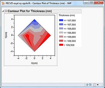
Thickness uniformity of test wafer using the test recipe
BPSG: RI vs. B/P EXPIRED!!!
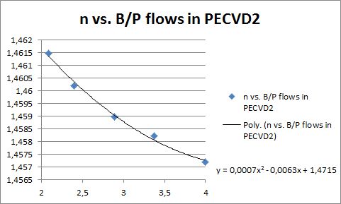
B2H6 flow and PH3 flow was varied to map the RI of different B2H6/PH3 ratios.
Work done by BGHE@dtu in fall 2013
| Recipe name | SiH4 flow [sccm] | N2O flow [sccm] | N2 flow [sccm] | B2H6 flow [sccm] | PH3 flow [sccm] | Pressure [mTorr] | Power [W] | Description |
| 1PBSG | 17 | 1600 | 0 | See below | See below | 500 | 800LF | BPSG glass for waveguide cladding layer |
LF=Low Frequency
| Run number | PH3 flow | B2H6 flow | B2H6/PH3 | RI | Thickness |
| A1 | 40 sccm | 135 sccm | 3.38 | 1.4582 | 3.28 µm |
| A2 | 55 sccm | 115 sccm | 2.09 | 1.4615 | 3.13 µm |
| A3 | 45 sccm | 130 sccm | 2.89 | 1.4590 | 3.13 µm |
| A4 | 35 sccm | 140 sccm | 4.0 | 1.4572 | 3.22 µm |
| A5 | 50 sccm | 120 sccm | 2.4 | 1.4602 | 3.14 µm |
Recipes on PECVD1 for deposition of silicon oxides EXPIRED!!!
Recipes
| Recipe name | SiH4 flow [sccm] | N2O flow [sccm] | N2 flow [sccm] | B2H6 flow [sccm] | PH3 flow [sccm] | GeH4*100 flow [sccm] | Pressure [mTorr] | Power [W] | Description |
| 1oxide/1ox_std/standard | 17 | 1600 | 0 | 0 | 0 | 0 | 400 | 380LF | Process control recipe. Developed for waveguides |
| 1PBSG | 17 | 1600 | 0 | 135 | 40 | 0 | 500 | 800LF | Developed for waveguide top cladding by Haiyan Ou @DTU Photonics'. |
| BGE_PBSG | 17 | 1600 | 0 | 240 | 60 | 0 | 500 | 800LF | Low stress PBSG |
| HO_core | 17 | 1600 | 300 | 0 | 0 | 400 | 400 | 600LF | Developed by Haiyan Ou @fotonik@dtu |
| HO_top | 17 | 1600 | 0 | 107 | 40 | 0 | 500 | 800LF | Developed by Haiyan Ou @fotonik@dtu |
Expected results
| Recipe name | Deposition rate [µm/min] | RI | Uniformity [%] | Comments |
| 1oxide/1ox_std/standard | ~0.193 | 1.46 | 2 | The latest measured values can be seen in the process control sheet in LabManager |
| 1PBSG | ~0.3 | 1.458@633nm |


