Specific Process Knowledge/Thin film deposition/Deposition of Silicon Oxide/Deposition of Silicon Oxide using PECVD/conformity
< Specific Process Knowledge | Thin film deposition | Deposition of Silicon Oxide | Deposition of Silicon Oxide using PECVD
Jump to navigation
Jump to search
Feedback to this page: click here
SiO2 deposition on holes with diameter 431nm-442nm and depth 257 nm
Work done by Lasse H. Thamdrup @Nilt on PECVD4 (added by bghe@nanolab) in January 2018
Information on Si wafer used for PECVD: Hole diameter d=431-442 nm and depth=257 nm.
The test wafer was scribed and broken into pieces. Deposition aiming at aprox. 100 nm SiO2 using recipe "Standard LF SiO2".
- Sample 1: 1min20s deposition time: Measured oxide thickness=103-104 nm.
- Sample 2: 6min45s deposition time- should be around 500 nm oxide.
Images: SEM3 of surface and cross-section by SEM2 conducted on test sample 1 and 2: The surface roughness has increased and the deposited SiO2 layer is not that conformal which results in reduced thickness on especially the sidewalls but also in the bottom of the holes- the thickness here is below half the thickness on the top.
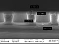
Sample 1 cross section

Sample 1 surface

Sample 2 cross section
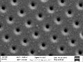
Sample 2 surface


