Specific Process Knowledge/Thermal Process/C1 Furnace Anneal-oxide: Difference between revisions
mNo edit summary |
|||
| Line 48: | Line 48: | ||
|- | |- | ||
!style="background:silver; color:black" align="center"|Performance | !style="background:silver; color:black" align="center"|Performance | ||
|style="background:LightGrey; color:black"|Film thickness | |style="background:LightGrey; color:black"|Film thickness and quality | ||
|style="background:WhiteSmoke; color:black"| | |style="background:WhiteSmoke; color:black"| | ||
*Dry SiO<sub>2</sub>: ~ 0 nm to 300 nm (it takes too long to grow a thicker dry oxide layers) | *Dry SiO<sub>2</sub>: ~ 0 nm to 300 nm (it takes too long to grow a thicker dry oxide layers) | ||
*Wet SiO<sub>2</sub>: ~ 0 nm to 3 µm (23 hours wet oxidation at 1100 <sup>o</sup>C) | *Wet SiO<sub>2</sub>: ~ 0 nm to 3 µm (23 hours wet oxidation at 1100 <sup>o</sup>C) | ||
* [[Specific Process Knowledge/Thermal Process/Oxidation/Breakdown voltage measurements/C1 furnace break-down voltage measurement results|Break-down voltage measurement results]] | |||
|- | |- | ||
!style="background:silver; color:black" align="center" valign="center" rowspan="3"|Process parameter range | !style="background:silver; color:black" align="center" valign="center" rowspan="3"|Process parameter range | ||
Latest revision as of 14:50, 16 September 2025
The content on this page, including all images and pictures, was created by DTU Nanolab staff, unless otherwise stated.
Feedback to this page: click here
Anneal-oxide furnace (C1)

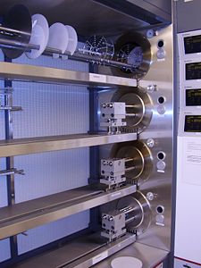
The Anneal-oxide furnace (C1) is a Tempress horizontal furnace for oxidation and annealing of silicon wafers. Both 100 mm and 150 mm wafers can be processed in the furnace.
The Anneal-oxide furnace is the top furnace tube in the C-stack furnaces, which positioned in cleanroom B-1. Most of wafers have to be RCA cleaned, before they enter the furnace. The only exceptions are brand new wafers, wafers from the A-stack furnaces, wafers from the LPCVD furnaces (B- and E-stack furnaces) and wafers from PECVD4. Please check the cross contamination information in LabManager, before you use the furnace.
Oxygen is used as oxidant for dry oxidation, and for wet oxidation wafer vapour generated by a steamer is used as oxidant. The oxidation recipes on the furnace are named e.g. "WET1000" and "DRY1000", where "WET" or "DRY" indicates whether it is a wet or dry oxidation process, and the number indicates the oxidation temperature.
Annealing can be done for silicon wafers with layers of e.g. silicon oxide, silicon nitride, polysilicon or BPSG glass (deposited in PECVD4). The annealing recipes are named e.g. "ANN1000" (for annealing at 1000 oC).
The oxidation and annealing temperature can be up to 1100 oC.
The user manual, technical information and contact information can be found in LabManager:
Process knowledge
- General information about oxidation. More information can be found on the oxidation page
- Wet oxidation in the C1 furnace. More information can be found here
- Dry oxidation in the C1 furnace. More information can be found here
- Annealing. More information can be found on the annealing page
| Purpose |
|
Annealing:
Oxidation:
|
|---|---|---|
| Performance | Film thickness and quality |
|
| Process parameter range | Process Temperature |
|
| Process pressure |
| |
| Gas flows |
| |
| Substrates | Batch size |
|
| Substrate materials allowed |
|
