LabAdviser/Technology Research/Fabrication of Hyperbolic Metamaterials using Atomic Layer Deposition/TiO2 Q plates: Difference between revisions
| Line 32: | Line 32: | ||
|- | |- | ||
!1.1 | !1.1 | ||
| | |RCA clean | ||
| | |Before Si deposition in LPCVD furnace, the quartz (fused silica) wafers need to be cleaned | ||
|[[Specific_Process_Knowledge/ | |[[Specific_Process_Knowledge/Wafer_cleaning/RCA| RCA]] | ||
|[[image: | |[[image:Zero1.jpg|250x350px|center|]] | ||
|- | |- | ||
| Line 41: | Line 41: | ||
|- style="background:#BCD4E6; color:black" | |- style="background:#BCD4E6; color:black" | ||
!1.2 | !1.2 | ||
| | |LPCVD of Si | ||
| | |LPCVD deposition of 300 nm amorphous Si | ||
|[[Specific_Process_Knowledge/ | |[[Specific_Process_Knowledge/Thin_film_deposition/Furnace_LPCVD_PolySilicon| 6" LPCVD polysilicon furnace (E2)]]. | ||
|[[image: | |[[image:Zero2.jpg|250x350px|center|]] | ||
|- | |- | ||
|- | |- | ||
!1.3 | !1.3 | ||
| | |Si anisotropic wet etch | ||
| | |Removal of the Si from the back side of the wafer. | ||
| [[Specific_Process_Knowledge/Etch/ | | [[Specific_Process_Knowledge/Etch/KOH_Etch|KOH]]. | ||
|[[image: | |[[image:Image1_Si_on_SiO2.jpg|250x350px|center|]] | ||
|- | |- | ||
| Line 59: | Line 59: | ||
!1.4 | !1.4 | ||
|Plasma surface treatment | |Plasma surface treatment | ||
|To ensure that remainings | |To ensure that all organic remainings are gone, wafer is treated by O<sub>2</sub>/N<sub>2</sub> plasma. (Optional step) | ||
|[[Specific_Process_Knowledge/Lithography/Strip#Plasma_Asher_2| Plasma Asher 2]] | | | ||
[[Specific_Process_Knowledge/Lithography/Strip#Plasma_Asher_2| Plasma Asher 2]] | |||
<br clear="all" /> | |||
[[Specific_Process_Knowledge/Lithography/Strip#Plasma_asher| Plasma Asher 1]] | |||
<br clear="all" /> | |||
| | | | ||
|- | |- | ||
| Line 66: | Line 70: | ||
|- | |- | ||
!1.5 | !1.5 | ||
| | |E-beam lithography (EBL) | ||
| | |Spin-coating of CSAR resist to the thickness of 150 nm, followed by e-beam exposure. | ||
| | | | ||
[[Specific_Process_Knowledge/ | [[Specific_Process_Knowledge/Lithography/EBeamLithography/JEOL_JBX-9500FSZ|JEOL JBX-9500 Electron-beam]] | ||
<br clear="all" /> | <br clear="all" /> | ||
|[[image:Image2_ebeam_on_Si.jpg|250x350px|center]] | |||
|[[image: | |||
|- | |- | ||
|- | |- | ||
|- style="background:#BCD4E6; color:black" | |- style="background:#BCD4E6; color:black" | ||
!1.6 | !1.6 | ||
| | |Advanced Silicon Etching | ||
| | |Creating sacrificial silicon template. | ||
| | | | ||
[[Specific_Process_Knowledge/Etch/ASE_(Advanced_Silicon_Etch)|ASE]] | |||
<br clear="all" /> | |||
|[[image:Image3_ASE_of_SI.jpg|250x350px|center]] | |||
|- | |- | ||
|- | |- | ||
!1.7 | !1.7 | ||
|Scanning Electron Microscopy inspection | |Scanning Electron Microscopy inspection | ||
| | |The fabricated template inspects by SEM | ||
| | | | ||
[[Specific_Process_Knowledge/Characterization/SEM_Supra_1|SEM Supra 1]] | [[Specific_Process_Knowledge/Characterization/SEM_Supra_1|SEM Supra 1]] | ||
| Line 98: | Line 99: | ||
<br clear="all" /> | <br clear="all" /> | ||
[[Specific_Process_Knowledge/Characterization/SEM_Supra_3|SEM Supra 3]] | [[Specific_Process_Knowledge/Characterization/SEM_Supra_3|SEM Supra 3]] | ||
|[[image: | |[[image:Si_template_q_plates.jpg|250x350px|center]] | ||
|- | |- | ||
|- | |- | ||
|- style="background:#BCD4E6; color:black" | |- style="background:#BCD4E6; color:black" | ||
!1.8 | !1.8 | ||
| | |Plasma surface treatment | ||
| | |To ensure that all organic remainings are gone, template is treated by O<sub>2</sub>/N<sub>2</sub> plasma. (Optional step) | ||
| | |||
[[Specific_Process_Knowledge/Lithography/Strip#Plasma_Asher_2| Plasma Asher 2]] | |||
<br clear="all" /> | |||
[[Specific_Process_Knowledge/Lithography/Strip#Plasma_asher| Plasma Asher 1]] | |||
<br clear="all" /> | |||
| | |||
|- | |- | ||
| Line 113: | Line 120: | ||
|- | |- | ||
!1.9 | !1.9 | ||
|Atomic Layer Deposition of TiO<sub>2</sub> | |||
|Deposition carried at 150C.Thickness is approx. 90 nm. | |||
||Equipment used: [[Specific_Process_Knowledge/Thin_film_deposition/ALD_Picosun_R200|ALD Picosun R200]]. Standard recipe used: [[Specific_Process_Knowledge/Thin_film_deposition/ALD_Picosun_R200/TiO2_deposition_using_ALD#TiO2_deposition_on_trenches| TiO2T]] . | |||
|[[image:Image4_ALD_of_SI_template.jpg|250x350px|center]] | |||
|- | |||
|- | |||
|- style="background:#BCD4E6; color:black" | |||
!1.10 | |||
|Ion beam etching (IBE). | |||
|Opening of deposited TiO<sub>2</sub> top layer using recipe [[Specific_Process_Knowledge/Etch/IBE⁄IBSD_Ionfab_300/IBE_Ti_etch|"Ti acceptance"]] there the stage was placed to 0<sup>o</sup> degree. The back side of the wafer also needs to be exposed to etching. | |||
|[[Specific_Process_Knowledge/Etch/IBE⁄IBSD_Ionfab_300|IBE/IBSD Ionfab 300]] | |||
|[[image:Image5_ALD_Ar_sputtering.jpg|250x350px|center]] | |||
|- | |||
|- | |||
!1.11 | |||
|Scanning Electron Microscopy inspection | |Scanning Electron Microscopy inspection | ||
| | |SEM inspection of ALD deposition and IBE etching. | ||
| | | | ||
[[Specific_Process_Knowledge/Characterization/SEM_Supra_1|SEM Supra 1]] | [[Specific_Process_Knowledge/Characterization/SEM_Supra_1|SEM Supra 1]] | ||
| Line 121: | Line 147: | ||
<br clear="all" /> | <br clear="all" /> | ||
[[Specific_Process_Knowledge/Characterization/SEM_Supra_3|SEM Supra 3]] | [[Specific_Process_Knowledge/Characterization/SEM_Supra_3|SEM Supra 3]] | ||
|[[image: | |[[image:top_removal_q_plates.jpg|250x350px|center]] | ||
|- | |- | ||
|- | |- | ||
|- style="background:#BCD4E6; color:black" | |- style="background:#BCD4E6; color:black" | ||
!1. | !1.12 | ||
|Selective etch of Si between ALD | |Selective etch of Si between ALD TiO<sub>2</sub> coatings. | ||
|Si etching proceeds using | |Si etching proceeds using Reactive Ion Etching (RIE) with isotropic process based on SF<sub>f</sub> process gas. | ||
||Equipment used: [[Specific_Process_Knowledge/Etch/ | ||Equipment used: [[Specific_Process_Knowledge/Etch/RIE_(Reactive_Ion_Etch)|RIE2]]. | ||
|[[image:Image6_ALD_Final_structure.jpg|250x350px|center]] | |||
|- | |- | ||
|- | |- | ||
!1. | !1.13 | ||
|Scanning Electron Microscopy inspection of fabricated structure. | |Scanning Electron Microscopy inspection of fabricated structure. | ||
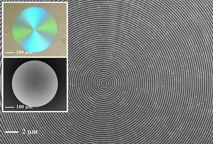
|Proof of final result. | |Proof of final result. | ||
| Line 144: | Line 170: | ||
<br clear="all" /> | <br clear="all" /> | ||
[[Specific_Process_Knowledge/Characterization/SEM_Supra_3|SEM Supra 3]] | [[Specific_Process_Knowledge/Characterization/SEM_Supra_3|SEM Supra 3]] | ||
|[[image: | |[[image:Si_removal_q_plates.jpg|250x350px|center]] | ||
|- | |- | ||
|- | |- | ||
|} | |} | ||
<br clear="all" /> | <br clear="all" /> | ||
Revision as of 16:23, 14 March 2017
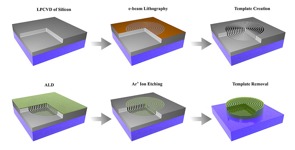
Procces flow description
The substrates for the samples were fabricated by depositing 1 μm of Si3N4 (the resonator layer) on 100 mm silicon < 100 > wafers using low-pressure chemical vapor deposition. The process was carried out at 780C with ammonia (NH3) and dichlorosilane (SiH2Cl2) as reactive gases. Thickness and refractive index of the deposited silicon nitride was measured and confirmed using spectroscopic ellipsometry. The deposited Si3N4 film was carefully analyzed for existence of cracks, particles and other defects using dark field optical microscopy. The best-quality wafer with Si3N4 was selected and cleaved in pieces, which were used as substrates for the deposition of Al2O3/TiO2 multilayers. Before inserting each substrate into the ALD reactor, it was placed on a Si carrier wafer. Therefore the Al2O3/TiO2 multilayers were grown not only on the Si3N4 layer but also on the dummy carrier wafer. After the ALD process was completed, the dummy was cleaved and its cross-section was characterized using scanning electron microscopy (SEM). The SEM images reveal high-quality homogeneous, conformal coatings, as seen in the examples in Figs 1. Such a method of deposited multilayers characterization turned out to be more feasible than the direct SEM characterization of multilayers on Si3N4, since the latter suffers from issues related to charge accumulation on the silicon nitride.
-
 High aspect ratio Al2O3 and TiO2 nanogratings.

-
 High aspect ratio Al2O3 and TiO2 nanogratings.
 -
 High aspect ratio Al2O3 and TiO2 nanogratings.


Process flow
Hej Evgeniy
Jeg har lagt dette eksemple på et process flow ind. Alt tekst og billeder skal selvfølgelig erstattes af relevante process steps for denne artikel.
Mvh. Berit
| Step | Description | LabAdviser link | Image showing the step | |
|---|---|---|---|---|
| 1.1 | RCA clean | Before Si deposition in LPCVD furnace, the quartz (fused silica) wafers need to be cleaned | RCA |  |
| 1.2 | LPCVD of Si | LPCVD deposition of 300 nm amorphous Si | 6" LPCVD polysilicon furnace (E2). |  |
| 1.3 | Si anisotropic wet etch | Removal of the Si from the back side of the wafer. | KOH. |  |
| 1.4 | Plasma surface treatment | To ensure that all organic remainings are gone, wafer is treated by O2/N2 plasma. (Optional step) | ||
| 1.5 | E-beam lithography (EBL) | Spin-coating of CSAR resist to the thickness of 150 nm, followed by e-beam exposure. |  | |
| 1.6 | Advanced Silicon Etching | Creating sacrificial silicon template. |  | |
| 1.7 | Scanning Electron Microscopy inspection | The fabricated template inspects by SEM |  | |
| 1.8 | Plasma surface treatment | To ensure that all organic remainings are gone, template is treated by O2/N2 plasma. (Optional step) | ||
| 1.9 | Atomic Layer Deposition of TiO2 | Deposition carried at 150C.Thickness is approx. 90 nm. | Equipment used: ALD Picosun R200. Standard recipe used: TiO2T . |  |
| 1.10 | Ion beam etching (IBE). | Opening of deposited TiO2 top layer using recipe "Ti acceptance" there the stage was placed to 0o degree. The back side of the wafer also needs to be exposed to etching. | IBE/IBSD Ionfab 300 |  |
| 1.11 | Scanning Electron Microscopy inspection | SEM inspection of ALD deposition and IBE etching. |  | |
| 1.12 | Selective etch of Si between ALD TiO2 coatings. | Si etching proceeds using Reactive Ion Etching (RIE) with isotropic process based on SFf process gas. | Equipment used: RIE2. |  |
| 1.13 | Scanning Electron Microscopy inspection of fabricated structure. | Proof of final result. |  | |