LabAdviser/Technology Research/Fabrication of Hyperbolic Metamaterials using Atomic Layer Deposition/TiO2 Q plates
Feedback to this page: click here
This page is written by Evgeniy Shkondin @DTU Nanolab if nothing else is stated.
All images and photos on this page belongs to DTU Nanolab and DTU Electro (previous DTU Fotonik).
The fabrication and characterization described below were conducted in 2013-2016 by Evgeniy Shkondin, DTU Nanolab.
Procces flow description
A 500 μm thick wafer of silica (SiO2) goes through RCA clean and low-pressure chemical vapor deposition (LPCVD) (furnace from Tempress) based on SiH4 (silane) at 560◦C to form a layer of 300 nm of amorphous silicon (Si) [Fig. 1]. The back side of deposited Si was etched using KOH wet etch. In order to remove residues from the etching process, it was performed oxygen plasma cleaning. A CSAR resist was spin-coated to the thickness of 150 nm, followed by exposure of Electron Beam Lithography (EBL) (JEOL JBX-9500 Electron-beam) generating a mask with concentric ring patterns. After development, the wafer was submitted to advanced silicon etch (ASE). To form the trenches of the TiO2 structures, a thin film of TiO2 was deposited using the ALD technique in a hot-wall system (Picosun R200), working with 2000 cycles at 150◦C [Fig.1]. The precursors used were titanium tetrachloride (TiCl4) and H2O (supplied by Strem Chemicals Equipment). The process was followed by Ar+ ion beam etching (IBE) on both sides of the wafer to remove excess of ALD deposited material. At the top most TiO2 layer the physical sputtering of the sample using Ar+ ions was performed in order to get access to Si core. On the backside, the Ar+ ions were used to remove the deposited TiO2. Finally, we performed a reactive ion etch on silicon, leaving only the TiO2 structures. The final system comprehends a base of SiO2 with nano-structures of TiO2 on it. Figure 2 shows the image of the system taken using scanning electron microscope (SEM) and conventional optical microscope. Figure 3 illustrates SEM cross-sectional image of the prepared Q-plate .

Figure 1. Scheme of fabrication flow.

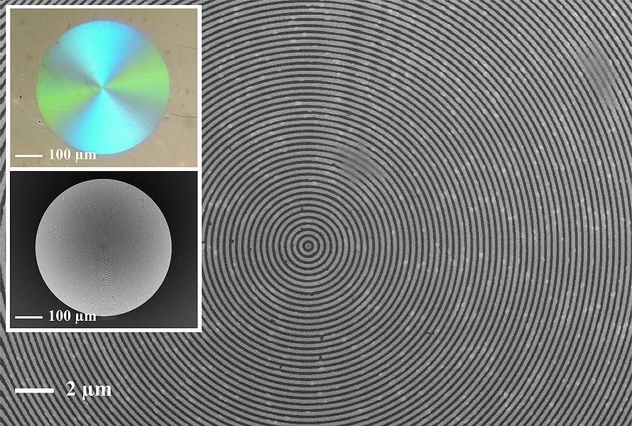
Figure 2. TiO2 concentric nanorings acting as a Q-plate. Insets show optical and SEM images of the whole plate.

Figure 3. Cross-sectional SEM image of the TiO2 Q-plate. a) The low magnification image shows the whole plate b) High magnification allows to inspect individual rings cross-sections.


Process flow
Description of steps for fabrication of Q-plates.
| Step | Description | LabAdviser link | Image showing the step | |
|---|---|---|---|---|
| 1.1 | RCA clean. | Before Si deposition in LPCVD furnace, the quartz (fused silica) wafers need to be cleaned | RCA |  |
| 1.2 | Low-Pressure Chemical Vapour Deposition (LPCVD) of Si. | LPCVD deposition of 300 nm amorphous Si | 6" LPCVD polysilicon furnace (E2). |  |
| 1.3 | Si anisotropic wet etch. | Removal of the Si from the back side of the wafer. | KOH. |  |
| 1.4 | Plasma surface treatment. | To ensure that all organic remainings are gone, wafer is treated by O2/N2 plasma. (Optional step) | ||
| 1.5 | E-Beam Lithography (EBL). | Spin-coating of CSAR resist to the thickness of 150 nm, followed by e-beam exposure. |  | |
| 1.6 | Advanced Silicon Etching. | Creating sacrificial silicon template. |  | |
| 1.7 | Scanning Electron Microscopy inspection. | The fabricated template inspects by SEM |  | |
| 1.8 | Plasma surface treatment. | To ensure that all organic remainings are gone, template is treated by O2/N2 plasma. (Optional step) | ||
| 1.9 | Atomic Layer Deposition (ALD) of TiO2. | Deposition carried at 150C.Thickness is approx. 90 nm. | Equipment used: ALD Picosun R200. Standard recipe used: TiO2T . |  |
| 1.10 | Ion Beam Etching (IBE). | Opening of deposited TiO2 top layer using recipe "Ti acceptance" there the stage was placed to 0o degree. The back side of the wafer also needs to be exposed to etching. | IBE/IBSD Ionfab 300 |  |
| 1.11 | Scanning Electron Microscopy inspection. | SEM inspection of ALD deposition and IBE etching. |  | |
| 1.12 | Selective etch of Si between ALD TiO2 coatings. (Reactive Ion Etching) | Si etching proceeds using Reactive Ion Etching (RIE) with isotropic process based on SF6 process gas. | Equipment used: RIE2. |  |
| 1.13 | Scanning Electron Microscopy inspection. | Proof of final result. |  | |