Specific Process Knowledge/Thin film deposition/ALD Picosun R200/TiO2 deposition using ALD
Feedback to this page: click here
This page is written by Evgeniy Shkondin @DTU Nanolab if nothing else is stated.
All images and photos on this page belongs to DTU Nanolab.
The fabrication and characterization described below were conducted in 2022 by Evgeniy Shkondin, DTU Nanolab.
Deposition of TiO2 is a standard, and well explored ALD process. Titanium(IV) isopropoxide (TTIP), Tetrakis(dimethylamido)titanium (TDMAT), and TiCl4 are the most popular. The last one is what is used at DTU Nanolab, because of the low cost and abundance. It can tolerate high temperatures (at least up to 500-550 °C) and can be employed for the deposition of TiO2 as well as TiN (in ALD-2). The only disadvantage is the minor chlorine contamination, especially pronounced at the lower temperature range (below 200 °C). The TiO2 film is very popular in many applications due to the ease of deposition, excellent uniformity, strict thickness control, and reliability. At DTU Nanolab you can either use ALD-1 or ALD-2 for the deposition of TiO2 with thermal (ALD-1 or ALD-2) or plasma (ALD-2) methods.
Unlike Al2O3, the TiO2 deposition process is quite complex. While increasing the temperature, the film will change the phase from amorphous to a polycrystalline (anatase) state. Typically users select an amorph layer if they need very smooth continuous films with high refractive index (many different photonic applications within waveguides and cavities). The refractive index for TiO2 is higher for polycrystalline anatase, but so also roughness. Anatase films are dominating in photovoltaics and solar cells relevant research. Another crystallographic phase known in TiO2 is rutile. This has an even higher refractive index but is unreachable with ALD as temperatures above 600 °C are usually required. It is possible to achieve a rutile form with plasma-enhanced ALD (PEAD) at a lower temperature but requires a biased stage which we do not have. If the rutile form is needed the users should consider reactive sputtering.
TiO2 ALD deposition using TiCl4 and H2O
TiO2 can be deposited in the range between 100 °C to 350 °C. The recommendation is to use 150 °C for amorphous TiO2 and 300-350 °C for anatase.
TiO2 recipes
Recipe: TiO2
Maximum deposition thickness: 100 nm
Temperature: 100 oC - 350 oC
| TiCl4 | H2O | |
|---|---|---|
| Nitrogen flow | 150 sccm | 200 sccm |
| Pulse time | 0.1 s | 0.1 s |
| Purge time | 4.0 s | 5.0 s |
This is a standard recipe of TiO2. It is suitable for coating the flat samples and structures with an aspect ratio of around up to 1:10.
Recipe: TiO2T
Maximum deposition thickness: 100 nm
Temperature: 100 oC - 350 oC
| TiCl4 | TiCl4 | H2O | H2O | |
|---|---|---|---|---|
| Nitrogen flow | 150 sccm | 150 sccm | 200 sccm | 200 sccm |
| Pulse time | 0.1 s | 0.1 s | 0.1 s | 0.1 s |
| Purge time | 0.5 s | 20.0 s | 0.5 s | 20.0 s |
This is a more complicated recipe that allows coating the sample with very high aspect ratio profiles. The recipe is good for deposition on very high aspect ratio structures (with aspect ratio more than 1:20) such as deep trenches, pillars, pores etc. TiO2T recipe can also be used for deposition on polymers at low temperatures (80-120 oC).
Deposition characteristics
The deposition rate for TiO2 depends on the temperature, see the ALD-window graph below. The uniformity, thickness, refractive index has been obtained using Ellipsometer VASE. Besides the temperature dependencies, the process exhibits a certain growth delay especially pronounced in the transition zone where the growth characteristics change significantly. This occurs in the temperature range where the phase shift from amorphous to polycrystalline (anatase) happens. Very interesting behavior observes between 200 °C and 250 °C. Here is a very abrupt change in the deposition rate present. To understand better this phenomenon, films with more dense temperature steps need to be deposited and analyzed.
Deposition rate

Deposition rate of TiO2 at 100 °C. Substrate: Silicon 4" wafer with native oxide.
. Here is no growth delay, but possibly a condensation phenomenon. This also means that this temperature is outside of the ALD window.
Deposition rate of TiO2 at 150 °C. Substrate: Silicon 4" wafer with native oxide.
. Growth delay is 18 cycles.
Deposition rate of TiO2 at 200 °C. Substrate: Silicon 4" wafer with native oxide.
. Growth delay is 30 cycles.
Deposition rate of TiO2 at 250 °C. Substrate: Silicon 4" wafer with native oxide.
. Growth delay is 194 cycles.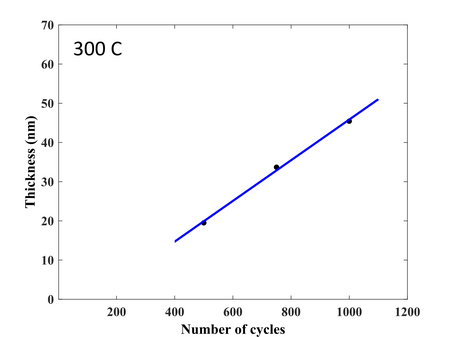
Deposition rate of TiO2 at 300 °C. Substrate: Silicon 4" wafer with native oxide.
. Growth delay is 116 cycles.
Deposition rate of TiO2 at 350 °C. Substrate: Silicon 4" wafer with native oxide.
. Growth delay is 84 cycles.
ALD window of TiO2. The deposition rate changes the behavior quite dramatically once the phase transition from amorphous to anatase starts. If the user wishes to deposit an amorph layer the 150C is the best choice. If anatase is desired the temperature should be 300C or 350C.

ALD window of TiO22O3. The nucleation and growth delay depend on the nature of the substrate, its crystallinity (amorph or crystal), and its chemical nature.


Uniformity across 100 mm wafer
Recipe "TiO2" Samples: 100mm ssp-Si
Results have been obtained for <100> 100 mm Si wafers with native oxide, based on ellipsometry study. Note, that for TiO2 a growth delay will occur, which can be quite pronounced depending on the selected temperature and substrate.
| Temperature (°C) / Number of cycles | Deposition rate (nm/s) | Average thickness (nm) | Standard deviation | Uniformity (%) |
|---|---|---|---|---|
| 100°C / 1000cycles | 0.0548 | 57.64 | 0.53 | 1.62 |
| 150°C / 1000cycles | 0.0462 | 45.02 | 0.46 | 1.87 |
| 200°C / 1000cycles | 0.0392 | 37.45 | 0.39 | 1.68 |
| 250°C / 1000cycles | 0.0600 | 48.36 | 0.28 | 0.94 |
| 300°C / 1000cycles | 0.0519 | 45.43 | 0.60 | 2.22 |
| 350°C / 1000cycles | 0.0455 | 41.57 | 0.28 | 0.95 |

Uniformity across 100mm wafer. Deposition at 100°C

Uniformity across 100mm wafer. Deposition at 150°C

Uniformity across 100mm wafer. Deposition at 200°C

Uniformity across 100mm wafer. Deposition at 250°C

Uniformity across 100mm wafer. Deposition at 300°C

Uniformity across 100mm wafer. Deposition at 350°C


Optical functions
TiO2 has been deposited on natively oxidized Si wafers (1000 cycles of TiCl4 and H2O) in the temperature range between 100°C and 350°C. The ellipsometry analysis is based on the Tauc-Lorentz model.

Refractive index of TiO2 deposited at different temperatures using 1000 cycles TiCl4 and H2O.

Absorption coefficient of TiO2 deposited at different temperatures using 1000 cycles TiCl4 and H2O.

Transmission intensity of 100 nm amorphous TiO2 vs. 100 nm anatase TiO2 (deposited on fused silica).


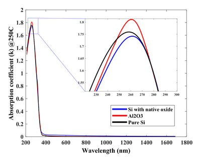
Optical functions of TiO2 deposited on different substrates
The physical properties of TiO2 are sensitive to the chemical and crystal nature of the substrate material it is deposited on. After all, ALD is a chemical reaction with the surface. Here the optical properties are shown for TiO2 deposited on Si with and without native oxide, as well as on Si with the 35 nm Al2O3. The nucleation and deposition rate are quite different on all three especially if the selected temperature is chosen to be in the transition zone of 150-250°C, where the phase change from amorphous to anatase polycrystals appear.

Refractive index. Deposition at 100°C

Refractive index. Deposition at 150°C

Refractive index. Deposition at 200°C

Refractive index. Deposition at 250°C

Refractive index. Deposition at 300°C

Refractive index. Deposition at 350°C


Absorption coefficient. Deposition at 100°C

Absorption coefficient. Deposition at 150°C

Absorption coefficient. Deposition at 200°C
Absorption coefficient. Deposition at 250°C

Absorption coefficient. Deposition at 300°C

Absorption coefficient. Deposition at 350°C


Deposition on flat samples (SEM inspection)
Surface morphology was inspected using SEM images. TiO2 layers were deposited on different substrates: Si without native oxide (HF-treated), Si with native oxide, and Si with 35 nm Al2O3 (300°C, 350 cycles). From the images, it is clearly visible that TiO2 growth and nucleation depend on the nature of the substrate surface used in the process. The difference is mainly pronounced in the transition zone region (200°C +/- 50°C), where the phase change appears.

TiO2 was deposited at 100°C and 1000 cycles using the standard “TiO2” recipe. Substarate: Si with native oxide.

TiO2 was deposited at 100°C and 1000 cycles using the standard “TiO2” recipe. Substarate: Pure Si (HF treated).

TiO2 was deposited at 100°C and 1000 cycles using the standard “TiO2” recipe. Substarate: Si with 35 nm Al2O3.

TiO2 was deposited at 150°C and 1000 cycles using the standard “TiO2” recipe. Substarate: Si with native oxide.

TiO2 was deposited at 150°C and 1000 cycles using the standard “TiO2” recipe. Substarate: Pure Si (HF treated).

TiO2 was deposited at 150°C and 1000 cycles using the standard “TiO2” recipe. Substarate: Si with 35 nm Al2O3.

TiO2 was deposited at 200°C and 1000 cycles using the standard “TiO2” recipe. Substarate: Si with native oxide.

TiO2 was deposited at 200°C and 1000 cycles using the standard “TiO2” recipe. Substarate: Pure Si (HF treated).

TiO2 was deposited at 200°C and 1000 cycles using the standard “TiO2” recipe. Substarate: Si with 35 nm Al2O3.

TiO2 was deposited at 250°C and 1000 cycles using the standard “TiO2” recipe. Substarate: Si with native oxide.

TiO2 was deposited at 250°C and 1000 cycles using the standard “TiO2” recipe. Substarate: Pure Si (HF treated).

TiO2 was deposited at 250°C and 1000 cycles using the standard “TiO2” recipe. Substarate: Si with 35 nm Al2O3.

TiO2 was deposited at 300°C and 1000 cycles using the standard “TiO2” recipe. Substarate: Si with native oxide.

TiO2 was deposited at 300°C and 1000 cycles using the standard “TiO2” recipe. Substarate: Pure Si (HF treated).

TiO2 was deposited at 300°C and 1000 cycles using the standard “TiO2” recipe. Substarate: Si with 35 nm Al2O3.

TiO2 was deposited at 350°C and 1000 cycles using the standard “TiO2” recipe. Substarate: Si with native oxide.

TiO2 was deposited at 350°C and 1000 cycles using the standard “TiO2” recipe. Substarate: Pure Si (HF treated).

TiO2 was deposited at 350°C and 1000 cycles using the standard “TiO2” recipe. Substarate: Si with 35 nm Al2O3.


Deposition on high aspect ratio structures (SEM inspection)
Titanium oxide has been deposited on Si trench structures to see the uniformity of the layer. The standard recipe “TiO2” was implemented. The trenches were inspected using SEM in cross-sectional mode. All samples were cut across the groves and along them, and all sides (across and along) were inspected.

Deposition of TiO2 on high aspect ratio Si trench structures. The trench height is 2000 nm. Deposition conditions: 300°C and 1000 cycles. A Standard “TiO2” recipe was used. Bird-eye-view.

Deposition of TiO2 on high aspect ratio Si trench structures. The trench height is 2000 nm. Deposition conditions: 300°C and 1000 cycles. A Standard “TiO2” recipe was used. Bird-eye-view.

Deposition of TiO2 on high aspect ratio Si trench structures. The trench height is 2000 nm. Deposition conditions: 300°C and 1000 cycles. A Standard “TiO2” recipe was used. Bird-eye-view.


Deposition of TiO2 on high aspect ratio Si trench structures. The trench height is 2000 nm. Deposition conditions: 100°C and 1000 cycles. A Standard “TiO2” recipe was used. Cutting direction: across the trench.

Deposition of TiO2 on high aspect ratio Si trench structures. The trench height is 2000 nm. Deposition conditions: 100°C and 1000 cycles. A Standard “TiO2” recipe was used. Cutting direction: across the trench.

Deposition of TiO2 on high aspect ratio Si trench structures. The trench height is 2000 nm. Deposition conditions: 100°C and 1000 cycles. A Standard “TiO2” recipe was used. Cutting direction: along the trench.

Deposition of TiO2 on high aspect ratio Si trench structures. The trench height is 2000 nm. Deposition conditions: 150°C and 1000 cycles. A Standard “TiO2” recipe was used. Cutting direction: across the trench.

Deposition of TiO2 on high aspect ratio Si trench structures. The trench height is 2000 nm. Deposition conditions: 150°C and 1000 cycles. A Standard “TiO2” recipe was used. Cutting direction: across the trench.

Deposition of TiO2 on high aspect ratio Si trench structures. The trench height is 2000 nm. Deposition conditions: 150°C and 1000 cycles. A Standard “TiO2” recipe was used. Cutting direction: along the trench.

Deposition of TiO2 on high aspect ratio Si trench structures. The trench height is 2000 nm. Deposition conditions: 200°C and 1000 cycles. A Standard “TiO2” recipe was used. Cutting direction: across the trench.

Deposition of TiO2 on high aspect ratio Si trench structures. The trench height is 2000 nm. Deposition conditions: 200°C and 1000 cycles. A Standard “TiO2” recipe was used. Cutting direction: across the trench.

Deposition of TiO2 on high aspect ratio Si trench structures. The trench height is 2000 nm. Deposition conditions: 200°C and 1000 cycles. A Standard “TiO2” recipe was used. Cutting direction: along the trench.

Deposition of TiO2 on high aspect ratio Si trench structures. The trench height is 2000 nm. Deposition conditions: 250°C and 1000 cycles. A Standard “TiO2” recipe was used. Cutting direction: across the trench.

Deposition of TiO2 on high aspect ratio Si trench structures. The trench height is 2000 nm. Deposition conditions: 250°C and 1000 cycles. A Standard “TiO2” recipe was used. Cutting direction: across the trench.

Deposition of TiO2 on high aspect ratio Si trench structures. The trench height is 2000 nm. Deposition conditions: 250°C and 1000 cycles. A Standard “TiO2” recipe was used. Cutting direction: along the trench.

Deposition of TiO2 on high aspect ratio Si trench structures. The trench height is 2000 nm. Deposition conditions: 300°C and 1000 cycles. A Standard “TiO2” recipe was used. Cutting direction: across the trench.

Deposition of TiO2 on high aspect ratio Si trench structures. The trench height is 2000 nm. Deposition conditions: 300°C and 1000 cycles. A Standard “TiO2” recipe was used. Cutting direction: across the trench.

Deposition of TiO2 on high aspect ratio Si trench structures. The trench height is 2000 nm. Deposition conditions: 300°C and 1000 cycles. A Standard “TiO2” recipe was used. Cutting direction: along the trench.

Deposition of TiO2 on high aspect ratio Si trench structures. The trench height is 2000 nm. Deposition conditions: 350°C and 1000 cycles. A Standard “TiO2” recipe was used. Cutting direction: across the trench.

Deposition of TiO2 on high aspect ratio Si trench structures. The trench height is 2000 nm. Deposition conditions: 350°C and 1000 cycles. A Standard “TiO2” recipe was used. Cutting direction: across the trench.

Deposition of TiO2 on high aspect ratio Si trench structures. The trench height is 2000 nm. Deposition conditions: 350°C and 1000 cycles. A Standard “TiO2” recipe was used. Cutting direction: along the trench.


X-ray photoelectron spectroscopy
XPS measurements of all samples has been performed using the XPS NEXSA equipment. The purpose of the investigation is to get an idea about the film stoichiometry, composition and possible contamination. Since the XPS NEXSA also offers REELS and ISS analysis these measurements were also performed.
The XPS Nexsa is equipped with the MAGCIS or Mono Atomic and Gas Cluster Ion Source that allows to sputter off material from the sample either using single argon atoms with energies up to 4 keV or by using ionized clusters of argon atoms (between 75 and 2000 atoms) with energies up to 8 keV. For this analysis, the native carbon contamination has been removed by Ar clusters at 4keV and a size of 300 atoms. The moisture level has been sputtered off by implementing 25 levels at 5 s each.
- MAGCIS cleaning of Al2O3 film surface

Removal of native carbon by Ar clusters.

Removal of native carbon by Ar clusters. 2D profile.


After the surface has been cleaned, the film has been measured, so the survey, valence region, and high-resolution elements (Ti, O, and Cl) scan have been acquired.

Survey scan.
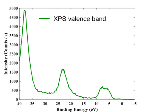
Valence region.


Ti 2p signal. High resolution scan. 100°C.

Ti 2p signal. High resolution scan. 150°C.

Ti 2p signal. High resolution scan. 200°C.

Ti 2p signal. High resolution scan. 250°C.

Ti 2p signal. High resolution scan. 300°C.

Ti 2p signal. High resolution scan. 350°C.

O 1s signal. High resolution scan. 100°C.

O 1s signal. High resolution scan. 150°C.

O 1s signal. High resolution scan. 200°C.

O 1s signal. High resolution scan. 250°C.

O 1s signal. High resolution scan. 300°C.

O 1s signal. High resolution scan. 350°C.

Cl 2p signal. High resolution scan. 100°C.

Cl 2p signal. High resolution scan. 150°C.

Cl 2p signal. High resolution scan. 200°C.

Cl 2p signal. High resolution scan. 250°C.

Cl 2p signal. High resolution scan. 300°C.

Cl 2p signal. High resolution scan. 350°C.


Stoichiometry results
| Stoichiometry results for TiO2 deposited with TiCl4 and H2O. | ||||||
|---|---|---|---|---|---|---|
| Temperature °C | 100 | 150 | 200 | 250 | 300 | 350 |
| Number of cycles | 1000 | 1000 | 1000 | 1000 | 1000 | 1000 |
| Ti (At. %) | 32.36 | 32.42 | 32.50 | 32.65 | 32.60 | 32.85 |
| O (At. %) | 65.57 | 66.68 | 66.98 | 67.35 | 67.40 | 67.15 |
| Cl (At. %) | 2.05 | 0.9 | 0.52 | 0 | 0 | 0 |
- Small amount of chlorine comes from unreacted TiCl4 processed at low temperatures.
REELS and ISS
Reflected Electron Energy Loss Spectroscopy (REELS) involves the exposure of the sample to a focused beam of monoenergetic electrons at 1keV coming from the flood gun. As these electrons interact with the material some of them will undergo inelastic scattering whereby they lose some kinetic energy. In reflection electron energy loss (REELS) the electrons that are both elastically and inelastically scattered are collected using the electron energy analyzer. The low-energy electron energy loss spectrum (up to ~50eV in energy loss) contains the elastic, or zero-loss, peak as well as the plasmon peaks. This spectrum can be used to determine information about the band structure and dielectric properties of the sample.
Calculated sampling depth for a 1 keV REELS experiment is ca. 15 nm, although it is noted that this will be dependent on the material being analyzed. Information from the REEL spectrum is complementary to other surface sensitive techniques, including XPS.
Ion scattering spectroscopy (ISS) is a technique in which a beam of He+ ions is scattered by a surface. The kinetic energy of scattered ions is measured; peaks are observed corresponding to elastic scattering of ions from atoms at the surface of the sample. Each element at the sample surface produces a peak at a different measured kinetic energy, caused by the momentum transfer between the incident ion and atom. The scattered ion and the scattering atom are normally of different masses, but the total momentum of the atom and ion is conserved. Therefore, as the initially "stationary" atom recoils, some kinetic energy is lost from the scattered ion, and the quantity of lost energy depends on the relative masses of the atom and ion. An ion scattering spectrum typically contains one peak for each element in the sample, with their separation in energy relating to the relative atomic masses of those elements. In some cases, different isotopes of the same element can be resolved, although this usually requires a primary ion heavier than He+. Strong scattering signals are limited to the topmost layer of atoms, so ISS is extremely surface-sensitive. Therefore, the sample must be clean, and even a small quantity of surface contaminant can significantly influence the ion scattering spectrum. Find more information here: https://www.thermofisher.com/dk/en/home/materials-science/learning-center/surface-analysis.html
ISS

ISS spectrum. (low current, Beam energy: 1kEv)

ISS spectrum. (low current, Beam energy: 1kEv)

ISS spectrum. (low current, Beam energy: 1kEv)

ISS spectrum. (low current, Beam energy: 1kEv)

ISS spectrum. (low current, Beam energy: 1kEv)

ISS spectrum. (low current, Beam energy: 1kEv)

ISS spectrum. (low current, Beam energy: 1kEv)


REELS

REELS spectrum

REELS spectrum

REELS spectrum

REELS spectrum

REELS spectrum

REELS spectrum


X-ray Reflectivity and Diffraction
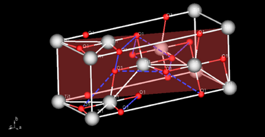
The crystal model of anatase TiO2. The transparent red plane across the lattice represents the 101 plane.

X-ray methods have also been involved in TiO2 characterization. The reflectivity method will allow measuring the film density and possible fluctuation of the density through the film thickness. The thickness and roughness can also be calculated. The grazing incidence diffraction can be applied to evaluate crystallinity in films prepared at different temperatures.
XRR analysis
X-ray reflectivity analysis (XRR) of samples (deposited at 150°C and 350°C) have been performed to investigate the thicknesses, roughness, and density profiles.
Three samples have been analyzed. 100 nm TiO2 deposited at 350°C, 100 nm TiO2 deposited at 150°C and 1000 cycles (45 nm) TiO2 deposited at 150°C on an amorph Al2O3 interlayer.
The scans have been obtained using Rigaku XRD SmartLab equipment. The voltage and current settings for the Cu X-ray tube were standard 40kV and 30mA. The incident optics contained an IPS (incident parallel slit) adaptor with 5 ° Soller slit. Other slits: IS=0.03mm RS1=0.03mm and RS2=0.075mm. Step size: 0.01 and measurement time - 5s for each point. The fitting process was performed using commercial GlobalFit software assuming the model based on Si or SiO2 substrates with native oxide/interlayer followed by the deposited TiO2 film and moisture surfaces. The results are summarized in the tables below.

Anatase TiO2 deposited at 350°C and 2174 cycles (approx. 100 nm) Profiles show almost invisible and heavily damped fringes. This corresponds to a high roughness, caused by the polycrystalline nature of the TiO2 layer where grain boundaries are quite pronounced.


Amorphous TiO2 deposited at 150°C and 2161 cycles (approx. 100 nm). Profiles show clear fringes that remain visible even at the high 2theta angle. This corresponds to a lower roughness.


Amorphous TiO2 deposited at 150°C and 1000 cycles (approx. 100 nm) deposited on a 35 nm Al2O3. The fringe profiles become quickly erratic, but still possible to fit.

| XRR results for TiO2 layers | |||||||||||||||||||||||||||||||||||||||||||||||||||||||||||||||||||||||||||||||||||||||||||||||||||||||||||||||||||||||||||||||||||||||||||||||||||||||||||||||||||||||||||||||||||||||||||
| |||||||||||||||||||||||||||||||||||||||||||||||||||||||||||||||||||||||||||||||||||||||||||||||||||||||||||||||||||||||||||||||||||||||||||||||||||||||||||||||||||||||||||||||||||||||||||


Grazing incidence X-ray diffraction (GiXRD)
The grazing incidence X-ray Diffraction (GiXRD) technique was applied to measure 100 nm TiO2 film deposited at 150°C and 350°C. The scans have been obtained using Rigaku XRD SmartLab equipment. The voltage and current settings for the Cu X-ray tube were standard 40kV and 30mA. The incident optics contained an incident parallel slit adaptor with incident 5 ° Soller slit. Receiving optics also included 5 ° Soller slit and parallel slit analyzer of 0.5 °. Other slits: IS=0.5mm RS1=open and RS2=open. Step size: 0.05 and measurement speed - 1° /min for each point. The measurement range was from 20 ° to 110 ° of 2θ. The incident angle was fixed at 2°.

GiXRD spectra of amorph (150°C) and anatase (350°C) TiO2 films. The diffraction pattern of the anatase form is in agreement with the COD database.
