Specific Process Knowledge/Lithography/EBL
Feedback to this page: click here
Quick links
My first JEOL 9500 exposure tutorial
JEOL 9500 trouble shooting guide
Introduction to E-beam lithography at DTU Nanolab
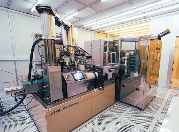
DTU Nanolab has two E-beam writing systems, a JEOL JBX-9500 FSZ and a Raith eLINE Plus. The two systems are very different and new users should consult the EBL team to dertermine which system is appropriate for a particular project or type of sample. The general specifications of the two tools are given in the table below and may serve as a guideline for choice of system to use, especially the pros and cons list at the end of the table. Newcommers to EBL should start by watching our JEOL 9500 process video to see how a typical process is done.
Compared to UV lithography EBL is somewhat more complicated and in general a significantly longer process. Writing time (per area) is much higher and thus EBL is only adviseable for structures with Critical Dimensions (CD) below 1 µm. For CD equal to or higher than 1 µm please consider our Maskless Aligner tools.
For more information and specific workflows on either tool, please refer to their respective pages; JEOL JBX-9500FSZ or Raith eLINE Plus.
Getting started and training in E-Beam Lithography
The JEOL 9500 system has a fairly steep learning curve and the information below and corresponding links are fairly comprehensive and describes uses and options that first time users of the JEOL 9500 system should not venture into. Instead, first time users of the JEOL 9500 system should consult our dedicated My First JEOL 9500 Exposure guide which showcases a JEOL 9500 job from start to finish in a tutorial form.
Please request training in E-Beam lithography by sending an email with your process flow to training@nanolab.dtu.dk.
JEOL 9500 and Raith eLine Plus specifications
| EBL system comparison table | |||
|---|---|---|---|
| Equipment | JEOL JBX-9500FSZ | Raith eLINE Plus | |
| Performance | Resolution | 8 nm | 35 nm |
| Maximum writing field | 1mm x 1mm | 1mm x 1mm | |
| Process parameter range | Acceleration voltage | 100 kV | 1-30 kV |
| Scan speed | 100 MHz | 20 MHz | |
| Min. electron beam size | 4 nm | 10 nm | |
| Min. step size | 0.25 nm | 1 nm | |
| Beam current range | 0.1 nA to 100 nA | 0.01 to 12 nA | |
| Minimum dwell time | 10 ns | 50 ns | |
| Samples | Batch size |
Wafer cassettes:
|
|
| Substrate material allowed |
|
| |
| General considerations | Pros |
|
|
| Cons |
|
| |
Fundementals of EBL pattern writing
Writing principle
Both of our EBL systems lets the user define a desired area dose to expose the resist with. Based on the beam current the systems will then calculate the necessary beam dwell to achieve the requested dose in the drawn areas. It is always the drawn (filled) parts of a pattern that will get exposed. In addition to area dose the Raith eLine tool allows the user to define a line dose for exposure of single lines. The JEOL 9500 system does not allow that.
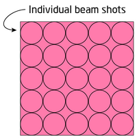
Before the pattern is exposed onto the substrate the pattern is broken down (fractured) into simple trapezoids and each trapezoidal shape is filled with beam shots, i.e. individual beam positions that together will make up the pattern. This is illustrated below with a simple pattern consisting of a square. The actual beam spot size is dependent on beam current and the pitch between beam positions is (within certain limitations) defined by the user.

|
|
Simple shape filled in with beam shots. |
The electron source is continuously emitting electrons and exposure of the beam towards the sample is controlled by a beam blanker. The position of the beam is controlled by the beam deflector and scanning coils. The pattern is written one beam shot at a time in a serial process as this
- Beam positioning for 1st beam position of current trapezoidal shape
- Unblank the beam
- Exposure
- Reposition for next beam shot
- Blank the beam at end of trapezoidal shape
Steps 2.1 and 2.2 continues in a loop until all beam shots of the current trapezoidal shape has been executed after which the beam is blanked and the system moves on to the next trapezoidal shape. It is obvious that exposure in such a way is relatively slow and has an overhead on top of the actual exposure time since time is also spent on beam positioning and blanking/unblanking the beam.
Exposure grid and exposure field
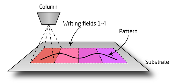
Both systems have a maximum writing field size of 1000 x 1000 µm2 since the deflection of the beam is limited to ±500 µm in both x- and y-direction. Patterns inside a writing filed is written by beam deflection only and hence the substrate stage remains stationary. Geometry larger than a single writing field will be fractured across multiple writing fields and hence between fields the substrate stage will move to reposition the substrate directly under the column as illustrated below.

|
|
Illustration of a waveguide spanning four exposure fields. Between fields the stage will reposition the substrate below the column. |
If neighbouring writing fields are not properly aligned features fractured across multiple writing fields may suffer from stitching errors, i.e. pattern discontinuities where the patterns do not align properly to each other. On the JEOL system write field alignment is ensured by a fully automated calibration sequence using internal alignment features. This ensures field stitching usually on the order of 10-15 nm or less. On the Raith system write field alignment is performed on the users own substrate and accuracy can vary.
The beam shots described above are placed onto the systems exposure grid, hence the resolution of beam shot placement is governed by the exposure grid. The resolution of this grid is determined by the positioning DAC of the system, on the JEOL 9500 this is 20 bit and on the Raith eLine it is 16 bit. Hence the JEOL 9500 system has in principle 220 = 1.048.576 grid positions along each axis while the Raith system has 216 = 65.384 grid positions along each axis. This means the JEOL system can maintain a 1 nm exposure grid over the entire 1000 x 1000 µm2 writing field whereas the Raith tool will have a 16 nm exposure grid at the maximum writing field.
Generalized workflow
While the EBL workflow resembles that of UV lithography there are a few additional complications and the parameter space is somewhat larger. The complications all arise from using electrons rather than light for exposure. Since a beam of electrons is used for exposure the substrate must be sufficiently conductive and grounded in order not to build up a charge. If the substrate in itself is not conductive a thin metal film or other conductive surface layer must be applied to it, read more on this in the resist section. Another complication is secondary exposure from backscattered electrons. This is a much bigger topic and covered in the pattern preparation section. A generalised workflow is shown below.
Since substrate preparation and development processes are (nearly) identical for the JEOL and Raith eLine systems they are described in common below. Pattern preparation, job preparation and job execution are fairly different between the two tools and hence these steps are described on the specific tool pages.
Substrate preparation
Substrates must be prepared for EBL bla blah. Read more on the EBL substrate preparation guide
Pattern preparation
Pattern preparation is somewhat different depending on if a pattern is exposed on JEOL 9500 or Raith eLine Plus. Please refer to the correct pattern preparation section below.
Pattern preparation for exposure on JEOL 9500.
Pattern preparation for exposure on Raith eLine Plus.
Job preparation
Job preparation is also different depending on if a pattern is exposed on JEOL 9500 or Raith eLine Plus. Please refer to the correct job preparation section below.
Job preparation for exposure on JEOL 9500.
Job preparation for exposure on Raith eLine Plus.
Job execution
Job execution is covered by the respective tool usage manuals found here
Development
AR 600-546 and ZED N-50 developers are available in a semi automatic puddle developer Developer: E-beam in E-4, mainly intended for development of AR-P 6200 and ZEP 520A. It has automatic recipes for puddle development cycles for 10, 30 and 60 seconds of either of the two developers, each finishing off with an IPA rinse and drying cycle. The system can handle chips, 2", 4" and 6" wafers.
Other resist have to be developed in the E-beam developer fumehood in E-4 in beakers. Please notice there are specific beaker sets for alkaline developers and for solvent based developers.
Post development inspection
After development it is often necesarry to evaluate the result by SEM to verify feature dimensions. This can conviently be done in the Raith eLine Plus tool which apart from being an EBL tool is also a semiautomatic SEM. The strong suit of the tool is the ability to link/align a design file to the substrate and simply define image positions in the design file. The user can then set up a long list of image locations and the tool will acquire the SEM images without further user input. When set up correctly the system can acquire about one image per 5 seconds which is very advantageous for large arrays of structures. For an introduction to this, please refer to our automatic SEM introduction video.
After image acquisition the images can be semi automatically processed with ProSEM to determine feature sizes. For large image sets the software can generate an Excel sheet with various dimension outputs.
Literature on E-beam Lithography
- Handbook of Microlithography, Micromachining, and Microfabrication, Volume 1: Microlithography, P. Rai-Choudhury (Editor), chapter 2 (p 139 – 250). Link to book can be found here: http://www.cnf.cornell.edu/cnf_spietoc.html
- Lithography, Wiley, 2011: Chapter 3, Electron Beam Lithography by Stefan Landis: http://onlinelibrary.wiley.com/doi/10.1002/9781118557662.ch3/summary

