Specific Process Knowledge/Thin film deposition/Physimeca
The content on this page, including all images and pictures, was created by DTU Nanolab staff, unless otherwise stated.
Feedback to this page: click here
The Physimeca has been decomissioned and is no longer available.
Physimeca

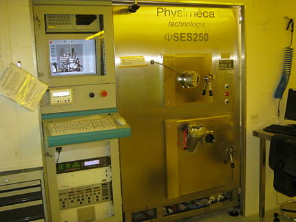
Physimeca is a system for deposition of metals through electron-beam evaporation.
Wafers are loaded into the system through the load lock and transferred into the deposition chamber. Physimeca allows you to deposit metals on samples up to 4 inch wafer. There are three different sample holders, one for chips (arbitrary size), one for 2" wafers and one for 4" wafers. The sample holder can be tilted during deposition, but is normally kept in a horizontal orientation.
Six different metals are present at each time in the Physimeca. The metal combination is changed if needed. A list of currently allowed metals is included in the table below; contact the ThinFilm team (Metal@nanolab.dtu.dk) if you have wishes for other metals.
The user manual and contact information can be found in LabManager:
| Purpose | Deposition of metals |
|
|---|---|---|
| Performance | Film thickness |
|
| Available metals and deposition rates (Å/s) |
| |
| Process parameter range | Process Temperature |
|
| Process pressure |
| |
| Distance between e-beam and substrate |
| |
| Substrates | Sample size |
|
| Substrate material allowed |
| |
| Materials allowed on the substrate |
|
* For thicknesses above 2000 Å special permission is required (contact thinfilm@nanolab.dtu.dk).
Calibration of Physimeca (experienced users only)
As of 16/6/2008, we will use a new system to compensate for "drift" without having to change e.g. 20 gold programs for each refilling. The power setting during deposition is a fraction of the "auto-emission current" on the genius system. In order to compensate for drift in the system the auto and max emission current on the genius is adjusted to achieve the rates at the set powers below This way it should not be necessary to adjust the programs every time, but experienced users will have to occasionally adjust the genius setting.
| Reference deposition (step) | Material | Rate (Å/s) | At power (%) | Example of max emission current (6-2008) | ||
| mA | ~mA for rate | |||||
| Ti100nm-5A-cal | Ti | 1 | 5 | 70 | 160 | 112 |
| Pt100nm-5A-cal | Pt | 2 | 5 | 80 | 460 | 368 |
| Au100nm-10A-cal | Au | 3 | 10 | 80 | 450 | 360 |
| Ni100nm-5A-cal | Ni | 4 | 5 | 70 | 250 | 175 |
| Ge100nm-5A-cal | Ge | 5 | 5 | 70 | 190 | 133 |
| Cr100nm-5A-cal | Cr | 6 | 5 | 70 | 110 | 77 |
| Pd100nm-5A-cal | Pd | 6 | 5 | 70 | 160 | 112 |
The tooling factor has been determined to ~110 for 100nm layers (lot, 6-2008). It will of course have a small dependence on material and rate.
You can use the steps above as starting point when making new programs (other thicknesses, rates, tilt etc.)
Changing Auto and Emission Current (experienced users only)
If the actual power during deposition is significantly different than the target value (e.g. off by a few % you may change the genius values).
Calculate new auto emission current: Inew="good" current during deposition / target power, e.g. 167mA/0.7 = 240mA (new max emission)
- Use genius remote:
- Switch to manual mode.
- Switch to chosen material
- Go to set data and down to auto emission and max emission .
- Change both to the new value and note this in the user log.
- Go to save/load and save values
- Switch back to remote mode on genius.
