Specific Process Knowledge/Etch/DRIE-Pegasus/Pegasus-4/SiO2 Etch/SiO2 etch with resist mask
Feedback to this page: click here
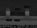
Design of experiment "DOE03" - SiO2 etch with DUV resist pattern
Done by Berit Herstrøm @DTU Nanolab Q1 2021
The design of the experiments "DOE03"
The design factors were:
- Coil power: 2500-4000 W
- Platen power: 200-300 W
- Total flow: 100-500 sccm
- He/C4F8 ratio: 5-30
- C4H8/H2 ratio: 1-3
Fixed settings were:
- Spacers used: 30 mm (DOE1 and DOE2 showed that 30mm spacer gave better selectivity to the resist than 100mm spacers)
- APC valve: 100% open (to keep pressure as low as possible) - Pressure will be very correlated to the total flow rate.
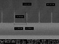
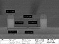
DOE03 run plan:
This has been designed in the software JMP PRO. Click on the image to make it larger.

Samples:
- One piece 2x2cm DUV patterened bond to a Si carrier wafer
- ~2µm SiO2 - ~90nm Barc, ~900nm Neg DUV resist - mask: Pegreticle
- Barc etch before the SiO2 etch: BarcO2 for 30 s
The responses I have evaluated are (See decriptions below):
- Etch rate of SiO2
- Etch rate selectivity to resist
- Etch profile angle in low aspect ratio areas
- Etch profile angle in higher aspect ratio areas
- Change in critical dimensions
- Aspect ratio dependent etch rate
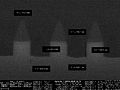
Results from the run of DOE03 - SiO2 etch with DUV resist pattern
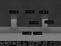
The DOE analysis of "DOE03"
Model of all responses together. Se explaination on the responses below.
- Here the responses are fittet one at a time (This gives better models for the individual responses but the overview is less good):
- Interactive HTM file: COPY THE HTM PATH INTO YOUR BROWSER, this will only work if you have acess to the Nanolab cleanroom drive - Try out the prediction profilers: file:///O:/CleanroomDrive/_Equipment/Pegasus%204/DOE3/Fit%20Model%20all%20responses%20individually%20fit%202.htm
- Inactive PDF file: File:Fit Model all responses individually fit.pdf
- Here they are fittet together (This gives a good overview but goes not give the best model each of the responses):
- Interactive HTM file: copy the link into your browser, this will only work if you have acess to the Nanolab cleanroom drive) - go to the bottom of the HTM page and try out the prediction profiler: file:///O:/CleanroomDrive/_Equipment/Pegasus%204/DOE3/Fit%20Model%20all%20responses%202.htm
- Inactive PDF file: File:Fit Model all responses 2.pdf
About the .htm interactive files: Copy the htm link into your browser and the document will open if you have access to the Cleanroom drive. The prediction profiler is interactive! Be aware that the resulting response from the prediction profiler might have large statistical uncertainty. Unfortunately the document does not include the coinfidence interval so you should only use it as guide lines. If you look at the below .pdf file for one selected set of parameters in the prediection profiler you can see the coenfidence interval for that set of factors.
Explanation of the responses that are included in the models:
Response Etch rate SiO2 in low aspect ratio: Etch rate in low aspect ratio areas
Here I have modelled the etch rate in the low aspect ration etched areas (4 µm pitch and 1 µm lines).
Response Selectivity: Etch rate selectivity to the resist
This is defined as the SiO2 etch rate in the low aspect ratio etched areas (4 µm pitch and 1 µm lines) devided by the resist etch rate also on the 1 µm lines in these areas.
Response SiO2 profile angle LAR: Etch profile angle in low aspect ratio etching
Modelling the etch profile angle is difficult because it depends on the aspect ratio of the etched structures. If the mask opening around the structure is small compared to the depth of the etch the aspect ratio is high. If the opening is large compared to the etch depth the aspect ratio is low. Here I have looked at low aspect ratio - more precisly I have looked at the profile of lines with 4 µm pitch and 1µm line width. The etch depth was been target to 1 µm. A different etch depth or a different starting thickness of the resist pattern will most likely give another profile angle.
Response SiO2 profile angle 1:1: Etch profile angle in 1:1 aspect ratio etching
Modelling the etch profile angle is difficult because it depends on the aspect ratio of the etched structures. If the mask opening around the structure is small compared to the depth of the etch the aspect ratio is high. If the opening is large compared to the etch depth the aspect ratio is low. Here I have looked at 1:1 aspect ratio - more precisly I have looked at the profile of lines with 2 µm pitch and 1 µm line width. The etch depth was been target to 1 µm. A different starting thickness of the resist pattern will most likely give another profile angle. I have not modelled higher aspect ratio structures since for the higher spect ratio structures in this study some of the samples has not been etched at all in the small opening and then the profile angle response cannot be modelled.
Respose ER 1:05/ER4:1: Aspect ratio dependent etch rate Different mask opening sizes etches with different rates - especially when the aspect ratio goes above 1 meaning the etch is deeper that the size of the opening. Here I have modelled the spect ratio dependant etch rate by modelling the ratio of the etch rate in the lines 4 µm pitch and 1 µm line over the etch rate in 1 µm pitch and 0.5µm lines. The etch depth in the large opening is about 1 µm.
Respose CD top/Bottomdifference: Change of critical dimensions (CD change)
Modelling the change in critical dimensions - that is the difference between the mask opening before etch and after etch. This has been measured as an average of the different size seen on the SEM images. It has been measured both in the top and the bottom. This modelling also includes the difference in CD change between top and bottom - this is actually another measure for the profile angle (negative value is positive tappered).
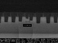
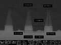
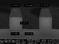
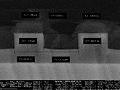
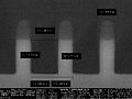
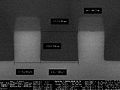
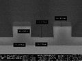
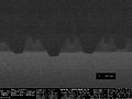
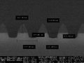
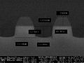
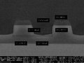
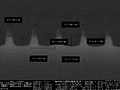
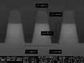
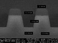
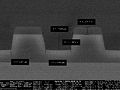
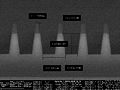
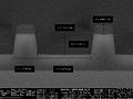
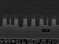
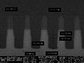
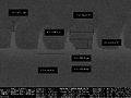
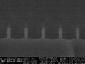
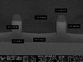
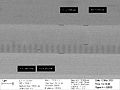
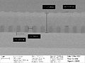
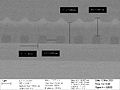
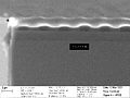
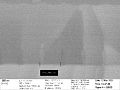
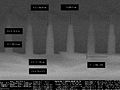
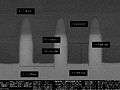
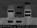
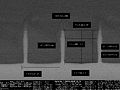
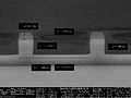
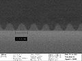
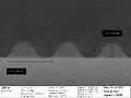
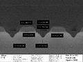
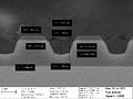
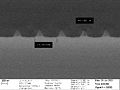
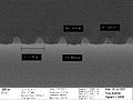
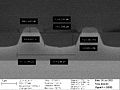
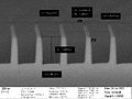
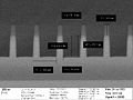
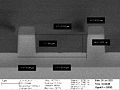
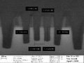
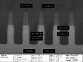
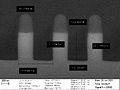
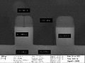
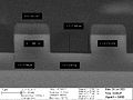
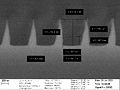
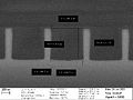
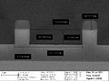
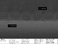
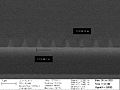
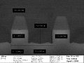
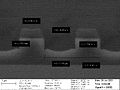
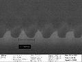
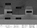
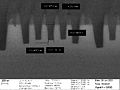
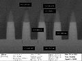
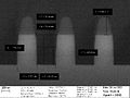
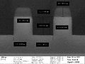
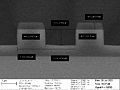
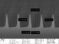
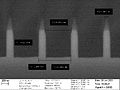
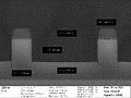
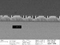
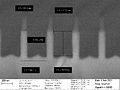
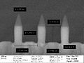
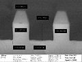
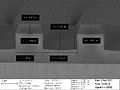
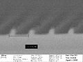
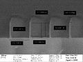
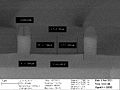
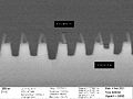
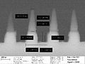
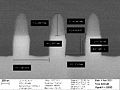
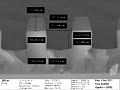
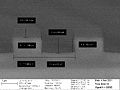
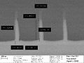
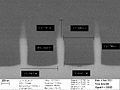
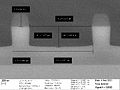
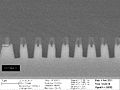
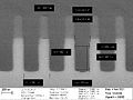
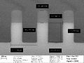
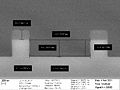
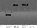
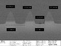
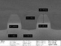
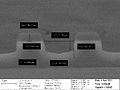
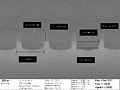
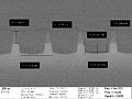
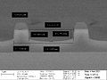
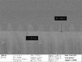
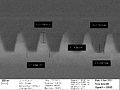
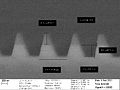
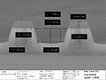
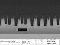
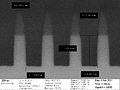
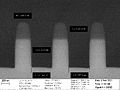
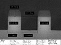
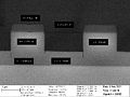
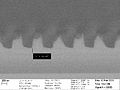
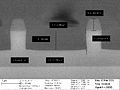
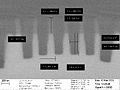
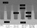
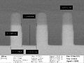
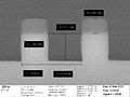
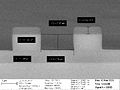
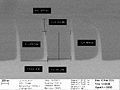
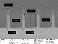
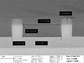
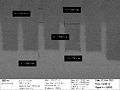
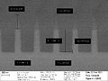
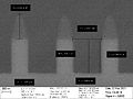
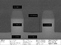
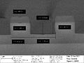
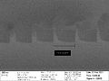
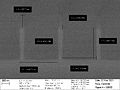
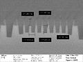
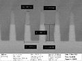
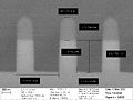
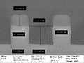
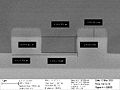
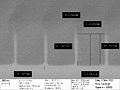
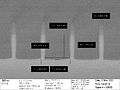
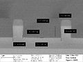
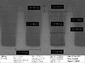
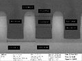
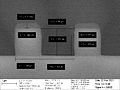
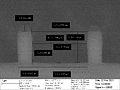
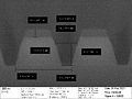
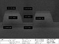
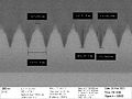
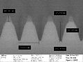
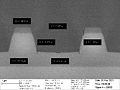
SEM images (All done by Berit Herstrøm, DTU Nanolab)
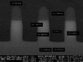
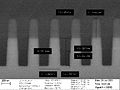
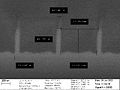
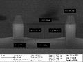
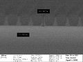
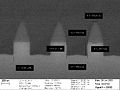
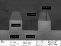
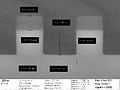
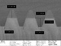
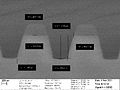
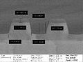
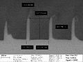
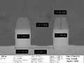
- Recipe no. 1: C06434_02 coil_3250W, platen:250W, He/C4F8= 17.5, C4F8/H2=2, Pressure:4.4mTorr C4F8:15.8sccm, He:276.3sccm, H2:7.9sccm, 4:51 min
-
 0.4µ/0.2µ
Bad pattern -
 0.5/0.25µ
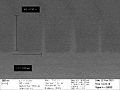
Etch depth: 125/95 nm
Resist left: 420 nm -
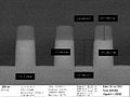
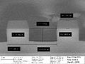
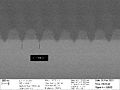
 1µ/0.5µ:
Etch depth: 587/569 nm
Resist left: 575 nm -
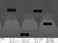
 2µ/1µ:
Etch depth: 823 nm
Resist left: 575 nm -
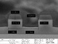
 4µ/2µ:
Etch depth: 923/1018 nm
Resist left: 688 nm -
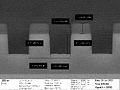
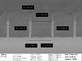
0.8µ/0.2µ
-
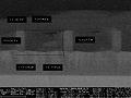 2.0µ/0.5µ:
Etch depth: 838/886 nm
Resist left: ? -
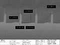
 4µ/1µ:
Etch depth: 988/1042 nm
Resist left: 612 nm


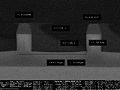
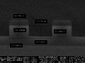
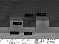
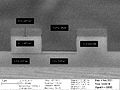
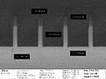
- Recipe no. 2: C06435_02 coil_3250W, platen:300W, He/C4F8= 30, C4F8/H2=3, Pressure:9.0mTorr, C4F8:16.0sccm, He:478.8sccm, H2:5.3sccm, 4:17 min
-
 0.4µ/0.2µ
Bad pattern -
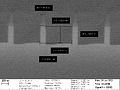
 0.5/0.25µ
Etch depth: 633/657 nm
Resist left: 417 nm -
 1µ/0.5µ:
Etch depth: 771/811 nm
Resist left: 476 nm -
 2µ/1µ:
Etch depth: 915 nm
Resist left: 449 nm -
 4µ/2µ:
Etch depth: 1063 nm
Resist left: 465 nm -
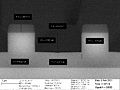
 0.8µ/0.2µ
 -
 1.0µ/0.25µ:
Etch depth: 862 nm
Resist left: 361 nm -
 4µ/1µ:
Etch depth: 969/1038 nm
Resist left: 446 nm


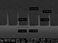
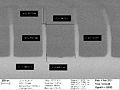
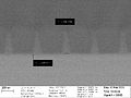
- Recipe no. 3: C06436_02 coil_4000W, platen:300W, He/C4F8= 5, C4F8/H2=3, Pressure:8.4mTorr, C4F8:78.9sccm, He:394.7sccm, H2:26.3sccm, 4:09 min
-
 0.4µ/0.2µ
Bad pattern -
 0.5/0.25µ
Etch depth: 0 nm
Resist left: ~350 nm -
 1µ/0.5µ:
Etch depth: 208/245 nm
Resist left: 486 nm -
 2µ/1µ:
Etch depth: 543/607 nm
Resist left: 490 nm -
 4µ/2µ:
Etch depth: 860/1020 nm
Resist left: 464 nm -
 0.8µ/0.2µ
Etch depth: 261/310 nm
Resist left: 280 nm -
 1.0µ/0.25µ:
Etch depth: 334/404 nm
Resist left: 371 nm -
 4µ/1µ:
Etch depth: 760/950 nm
Resist left: 501 nm


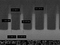
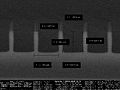
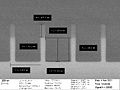
- Recipe no. 4: C06437_02 coil_2500W, platen:300W, He/C4F8= 5, C4F8/H2=1, Pressure:4.6mTorr, C4F8:42.9sccm, He:214.3sccm, H2:42.9sccm, 3:52 min
-
 0.4µ/0.2µ
Etch depth: 336 nm
Resist left: 411 nm -
 0.5/0.25µ
Etch depth: 453 nm
Resist left: 435 nm -
 1µ/0.5µ:
Etch depth: 717 nm
Resist left: 485 nm -
 2µ/1µ:
Etch depth: 883 nm
Resist left: 497 nm -
 4µ/2µ:
Etch depth: 1042 nm
Resist left: 470 nm -
 0.8µ/0.2µ
Etch depth: 776/850 nm
Resist left: 0 nm -
 1.0µ/0.25µ:
Etch depth: 757 nm
Resist left: 429 nm -
 4µ/1µ:
Etch depth: 1055 nm
Resist left: 465 nm


- Recipe no. 5: C06438_02 coil_4000W, platen:300W, He/C4F8= 30, C4F8/H2=1, Pressure:1.5mTorr, C4F8:3.1sccm, He:93.8sccm, H2:3.1sccm, 4:24 min
-
 0.4µ/0.2µ
 -
 0.5/0.25µ
Etch depth: 559 nm
Resist left: 417 nm -
 1µ/0.5µ:
Etch depth: 739 nm
Resist left: 522 nm -
 2µ/1µ:
Etch depth: 925 nm
Resist left: 491 nm -
 4µ/2µ:
Etch depth: 1001 nm
Resist left: 504 nm -
 0.8µ/0.2µ
Etch depth: 867 nm
Resist left: 338 nm -
 1.0µ/0.25µ:
Etch depth: 867 nm
Resist left: 386 nm -
 4µ/1µ:
Etch depth: 1016 nm
Resist left: 512 nm


- Recipe no. 6: C06441_02 coil_3250W, platen:200W, He/C4F8= 5, C4F8/H2=1, Pressure:1.7mTorr, C4F8:14.3sccm, He:71.4sccm, H2:14.3sccm, 5:07 min
-
0.4µ/0.2µ
-
 0.5/0.25µ
Etch depth: 0 nm
Resist left: nm -
 1µ/0.5µ:
Etch depth: 425 nm
Resist left: 593 nm -
 2µ/1µ:
Etch depth: 771 nm
Resist left: 607 nm -
 4µ/2µ:
Etch depth: 1044 nm
Resist left: 576 nm -
 0.8µ/0.2µ
Etch depth: 496 nm
Resist left: 288 nm -
 1.0µ/0.25µ:
Etch depth: nm
Resist left: nm -
 4µ/1µ:
Etch depth: 1100 nm
Resist left: 612 nm


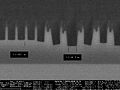
- Recipe no. 7: C06560_01 coil_4000W, platen:200W, He/C4F8= 5, C4F8/H2=1, Pressure:8.5mTorr, C4F8:71.4sccm, He:357.1sccm, H2:71.4sccm, 12:00 min
-
 0.4/0.2µ
Etch depth: 0 nm
Resist left: nm -
 0.5/0.25µ
Etch depth: 0 nm
Resist left: nm -
 1µ/0.5µ:
Etch depth: 0 nm
Resist left: nm -
 2µ/1µ:
Etch depth: 0 nm
Resist left: nm -
 4µ/2µ:
Etch depth: 0 nm
Resist left: nm -
 0.8µ/0.2µ
Etch depth: 0 nm
Resist left: nm -
 1.0µ/0.25µ:
Etch depth: 0 nm
Resist left: nm -
 4µ/1µ:
Etch depth: 0 nm
Resist left: nm


- Recipe no. 8: C06442_02 coil_4000W, platen:300W, He/C4F8= 5, C4F8/H2=2, Pressure:1.8mTorr, C4F8:15.4sccm, He:76.9sccm, H2:7.7sccm, 3:19 min
-
0.4µ/0.2µ
-
 0.5/0.25µ
Etch depth: 719 nm
Resist left: 265 nm -
 1µ/0.5µ:
Etch depth: 839 nm
Resist left: 487 nm -
 2µ/1µ:
Etch depth: 957 nm
Resist left: 474 nm -
 4µ/2µ:
Etch depth: 1048 nm
Resist left: 469 nm -
 0.8µ/0.2µ
Etch depth: nm
Resist left: nm -
 1.0µ/0.25µ:
Etch depth: 896 nm
Resist left: 184 nm -
 4µ/1µ:
Etch depth: 1088 nm
Resist left: 491 nm


- Recipe no. 9: C06444_02 coil_2500W, platen:200W, He/C4F8= 5, C4F8/H2=3, Pressure:8.9mTorr, C4F8:78.9sccm, He:394.7sccm, H2:26.3sccm, 3:19 min
-
0.4µ/0.2µ
-
 0.5/0.25µ
Etch depth: 0 nm
Resist left: nm -
 1µ/0.5µ:
Etch depth: 0 nm
Resist left: 339 nm -
 2µ/1µ:
Etch depth: 398 nm
Resist left: 345 nm -
 4µ/2µ:
Etch depth: 1032 nm
Resist left: 316 nm -
 0.8µ/0.2µ
Etch depth: 0 nm
Resist left: 232 nm -
 1.0µ/0.25µ:
Etch depth: 63 nm
Resist left: 280 nm -
 4µ/1µ:
Etch depth: 979 nm
Resist left: 358 nm


- Recipe no. 10: C06445_02 coil_2500W, platen:300W, He/C4F8= 17.5, C4F8/H2=1, Pressure:8.8mTorr, C4F8:25.6sccm, He:448.7sccm, H2:25.6sccm, 3:56 min
-
 0.4µ/0.2µ
 -
 0.5/0.25µ
Etch depth: 652 nm
Resist left: 456 nm -
 1µ/0.5µ:
Etch depth: 855 nm
Resist left: 487 nm -
 2µ/1µ:
Etch depth: 952 nm
Resist left: 487 nm -
 4µ/2µ:
Etch depth: 1106 nm
Resist left: 487 nm -
 0.8µ/0.2µ
Etch depth: 867 nm
Resist left: 426 nm -
 1.0µ/0.25µ:
Etch depth: 893 nm
Resist left: 460 nm -
 4µ/1µ:
Etch depth: 1033 nm
Resist left: 473 nm


- Recipe no. 11: C06446_02 coil_2500W, platen:200W, He/C4F8= 30, C4F8/H2=1, Pressure:1.5mTorr, C4F8:3.1sccm, He:93.8sccm, H2:3.1sccm, 5:38 min
-
 0.4µ/0.2µ
Etch depth: 552 nm
Resist left: 460 nm -
 0.5/0.25µ
Etch depth: 642 nm
Resist left: 469 nm -
 1µ/0.5µ:
Etch depth: 799 nm
Resist left: 528 nm -
 2µ/1µ:
Etch depth: 895 nm
Resist left: 548 nm -
 4µ/2µ:
Etch depth: 949 nm
Resist left: 536 nm -
 0.8µ/0.2µ
Etch depth: 840 nm
Resist left: 0? nm -
 1.0µ/0.25µ:
Etch depth: 814 nm
Resist left: ? nm -
 4µ/1µ:
Etch depth: 908 nm
Resist left: 542 nm


- Recipe no. 12: C06447_02 coil_4000W, platen:200W, He/C4F8= 30, C4F8/H2=2, Pressure:4.4mTorr, C4F8:9.6sccm, He:287.2sccm, H2:3.2sccm, 7:38 min
-
0.4µ/0.2µ
-
 0.5/0.25µ
Etch depth: 0 nm
Resist left: 304 nm -
 1µ/0.5µ:
Etch depth: 0 nm
Resist left: 547 nm -
 2µ/1µ:
Etch depth: 663 nm
Resist left: 631 nm -
 4µ/2µ:
Etch depth: 926 nm
Resist left: 667 nm -
 0.8µ/0.2µ
Etch depth: nm
Resist left: nm -
 1.0µ/0.25µ:
Etch depth: 577 nm
Resist left: 280 nm -
 4µ/1µ:
Etch depth: 1111 nm
Resist left: 648 nm


- Recipe no. 13: C06449_02 coil_2500W, platen:200W, He/C4F8= 30, C4F8/H2=2, Pressure:9.0mTorr, C4F8:15.9sccm, He:476.2sccm, H2: 7.9sccm, 7:10 min
-
0.4µ/0.2µ
-
 0.5/0.25µ
Etch depth: 0 nm
Resist left: 399 nm -
 1µ/0.5µ:
Etch depth: 318 nm
Resist left: 573 nm -
 2µ/1µ:
Etch depth: 683 nm
Resist left: 579 nm -
 4µ/2µ:
Etch depth: 1021 nm
Resist left: 604 nm -
 0.8µ/0.2µ
Etch depth: 426 nm
Resist left: 254 nm -
 1.0µ/0.25µ:
Etch depth: 513 nm
Resist left: 342 nm -
 4µ/1µ:
Etch depth: 995 nm
Resist left: 597 nm


- Recipe no. 14: C06450_02 coil_2500W, platen:250W, He/C4F8= 5, C4F8/H2=3, Pressure:1.6mTorr, C4F8:15.8sccm, He:78.9sccm, H2:5.3sccm, 3:51 min
-
 0.4µ/0.2µ
Etch depth: 496 nm
Resist left: 333 nm -
 0.5/0.25µ
Etch depth: 548 nm
Resist left: 405 nm -
 1µ/0.5µ:
Etch depth: 780 nm
Resist left: 468 nm -
 2µ/1µ:
Etch depth: 904 nm
Resist left: 462 nm -
 4µ/2µ:
Etch depth: 1080 nm
Resist left: 472 nm -
 0.8µ/0.2µ
Etch depth: 949 nm
Resist left: ? nm -
 1.0µ/0.25µ:
Etch depth: 828 nm
Resist left: 399 nm -
 4µ/1µ:
Etch depth: 1067 nm
Resist left: 495 nm


- Recipe no. 15: C06451_02 coil_4000W, platen:250W, He/C4F8= 30, C4F8/H2=1, Pressure:9.0mTorr, C4F8:15.6sccm, He:468.7sccm, H2:15.6sccm, 6:17 min
-
 0.4µ/0.2µ
Etch depth: 0 nm
Resist left: 0 nm -
 0.5/0.25µ
Etch depth: 468 nm
Resist left: 283 nm -
 1µ/0.5µ:
Etch depth: 652 nm
Resist left: 530 nm -
 2µ/1µ:
Etch depth: 857 nm
Resist left: 608 nm -
 4µ/2µ:
Etch depth: 1064 nm
Resist left: 601 nm -
 0.8µ/0.2µ
Etch depth: ? nm
Resist left: ? nm -
 1.0µ/0.25µ:
Etch depth: 733 nm
Resist left: 249 nm -
 4µ/1µ:
Etch depth: 1124 nm
Resist left: 601 nm


- Recipe no. 16: C06452_02 coil_4000W, platen:200W, He/C4F8= 17.5, C4F8/H2=3, Pressure:1.6mTorr, C4F8:5.3sccm, He:92.9sccm, H2:1.8sccm, 5:05 min
-
 0.4µ/0.2µ
Etch depth: nm
Resist left: nm -
 0.5/0.25µ
Etch depth: 227 nm
Resist left: 519 nm -
 1µ/0.5µ:
Etch depth: 567 nm
Resist left: 603 nm -
 2µ/1µ:
Etch depth: 844 nm
Resist left: 590 nm -
 4µ/2µ:
Etch depth: 1004 nm
Resist left: 593 nm -
 0.8µ/0.2µ
Etch depth: 689 nm
Resist left: 261 nm -
 1.0µ/0.25µ:
Etch depth: 767 nm
Resist left: 474 nm -
 4µ/1µ:
Etch depth: 1027 nm
Resist left: 598 nm


- Recipe no. 17: C06453_02 coil_2500W, platen:300W, He/C4F8= 30, C4F8/H2=3, Pressure:2.1mTorr, C4F8:4.7sccm, He:142.2sccm, H2:1.6sccm, 4:19 min
-
 0.4µ/0.2µ
Etch depth: 0 nm
Resist left: nm -
 0.5/0.25µ
Etch depth: 649 nm
Resist left: 440 nm -
 1µ/0.5µ:
Etch depth: 757 nm
Resist left: 468 nm -
 2µ/1µ:
Etch depth: 817 nm
Resist left: 473 nm -
 4µ/2µ:
Etch depth: 915 nm
Resist left: 494 nm -
 0.8µ/0.2µ
Etch depth: 799 nm
Resist left: 393 nm -
 1.0µ/0.25µ:
Etch depth: 786 nm
Resist left: 430 nm -
 4µ/1µ:
Etch depth: 869 nm
Resist left: 497 nm


- Recipe no. 18: C06454_02 coil_3250W, platen:250W, He/C4F8= 5, C4F8/H2=2, Pressure:4.6mTorr, C4F8:46.2sccm, He:230.8sccm, H2:23.1sccm, 5:16 min
-
0.4µ/0.2µ
-
 0.5/0.25µ
Etch depth: dep. nm
Resist left: 354 nm -
 1µ/0.5µ:
Etch depth: 122 nm
Resist left: 514 nm -
 2µ/1µ:
Etch depth: 489 nm
Resist left: 579 nm -
 4µ/2µ:
Etch depth: 850 nm
Resist left: 564 nm -
 0.8µ/0.2µ
Etch depth: 246 nm
Resist left: 280 nm -
 1.0µ/0.25µ:
Etch depth: 316 nm
Resist left: 363 nm -
 4µ/1µ:
Etch depth: 991 nm
Resist left: 591 nm


- Recipe no. 19: C06455_02 coil_3250W, platen:300W, He/C4F8= 5, C4F8/H2=1, Pressure:8.5mTorr, C4F8:71.4sccm, He:357.1sccm, H2:71.4sccm, 5:00 min
-
0.4µ/0.2µ
-
 0.5/0.25µ
Etch depth: 0 nm
Resist left: 383 nm -
 1µ/0.5µ:
Etch depth: 449 nm
Resist left: 433 nm -
 2µ/1µ:
Etch depth: 941 nm
Resist left: 461 nm -
 4µ/2µ:
Etch depth: 1287 nm
Resist left: 426 nm -
 0.8µ/0.2µ
Etch depth: 296 nm
Resist left: 362 nm -
 1.0µ/0.25µ:
Etch depth: 412 nm
Resist left: 404 nm -
 4µ/1µ:
Etch depth: 1075 nm
Resist left: 493 nm


- Recipe no. 20: C06456_02 coil_2500W, platen:250W, He/C4F8= 17.5, C4F8/H2=3, Pressure:8.8mTorr, C4F8:26.5sccm, He:464.6sccm, H2:8.8sccm, 4:32 min
-
 0.4µ/0.2µ
Etch depth: nm
Resist left: nm -
 0.5/0.25µ
Etch depth: 538 nm
Resist left: 447 nm -
 1µ/0.5µ:
Etch depth: 740 nm
Resist left: 450 nm -
 2µ/1µ:
Etch depth: 931 nm
Resist left: 429 nm -
 4µ/2µ:
Etch depth: 1076 nm
Resist left: 422 nm -
 0.8µ/0.2µ
Etch depth: 756 nm
Resist left: 330 nm -
 1.0µ/0.25µ:
Etch depth: 797 nm
Resist left: 392 nm -
 4µ/1µ:
Etch depth: 1092 nm
Resist left: 434 nm


- Recipe no. 21: C06475_01 coil_3250W, platen:200W, He/C4F8= 30, C4F8/H2=1, Pressure:4.4mTorr, C4F8:9.4sccm, He:281.3sccm, H2:9.4sccm, 6:51 min
-
0.4µ/0.2µ
-
 0.5/0.25µ
Etch depth: 0 nm
Resist left: 409 nm -
 1µ/0.5µ:
Etch depth: 589 nm
Resist left: 592 nm -
 2µ/1µ:
Etch depth: 874 nm
Resist left: 622 nm -
 4µ/2µ:
Etch depth: 1052 nm
Resist left: 666 nm -
 0.8µ/0.2µ
Etch depth: nm
Resist left: nm -
 1.0µ/0.25µ:
Etch depth: 876 nm
Resist left: 404 nm -
 4µ/1µ:
Etch depth: 1021 nm
Resist left: 631 nm


- Recipe no. 22: C06479_01 coil_3250W, platen:300W, He/C4F8= 17.5, C4F8/H2=2, Pressure:1.5mTorr, C4F8:5.3sccm, He:92.1sccm, H2:2.6sccm, 4:12 min
-
 0.4µ/0.2µ
Etch depth: 561 nm
Resist left: 404 nm -
 0.5/0.25µ
Etch depth: 629 nm
Resist left: 412 nm -
 1µ/0.5µ:
Etch depth: 786 nm
Resist left: 473 nm -
 2µ/1µ:
Etch depth: 901 nm
Resist left: 508 nm -
 4µ/2µ:
Etch depth: 1017 nm
Resist left: 462 nm -
 0.8µ/0.2µ
Etch depth: 830 nm
Resist left: 368 nm -
 1.0µ/0.25µ:
Etch depth: 877 nm
Resist left: 427 nm -
 4µ/1µ:
Etch depth: 976 nm
Resist left: 495 nm


- Recipe no. 23: C06480_01 coil_4000W, platen:300W, He/C4F8= 17.5, C4F8/H2=2, Pressure:4.4mTorr, C4F8:15.8sccm, He:276.9sccm, H2:7.9sccm, 4:08 min
-
 0.4µ/0.2µ
Etch depth: 505 nm
Resist left: 262 nm -
 0.5/0.25µ
Etch depth: 594 nm
Resist left: 359 nm -
 1µ/0.5µ:
Etch depth: 766 nm
Resist left: 550 nm -
 2µ/1µ:
Etch depth: 914 nm
Resist left: 550 nm -
 4µ/2µ:
Etch depth: 1059 nm
Resist left: 552 nm -
 0.8µ/0.2µ
Etch depth: nm
Resist left: nm -
 1.0µ/0.25µ:
Etch depth: 862 nm
Resist left: 396 nm -
 4µ/1µ:
Etch depth: 1050 nm
Resist left: 564 nm


- Recipe no. 24: C06559_01 coil_4000W, platen:300W, He/C4F8= 30, C4F8/H2=3, Pressure:2.1mTorr, C4F8:4.7sccm, He:142.2sccm, H2:1.6sccm, 4:20 min
-
 0.4/0.2µ
Etch depth: 465 nm
Resist left: 406 nm -
 0.5/0.25µ
Etch depth: 542 nm
Resist left: 457 nm -
 1µ/0.5µ:
Etch depth: 745 nm
Resist left: 532 nm -
 2µ/1µ:
Etch depth: 887 nm
Resist left: 530 nm -
 4µ/2µ:
Etch depth: 1001 nm
Resist left: 532 nm -
 0.8µ/0.2µ
Etch depth: 826 nm
Resist left: 260 nm -
 1.0µ/0.25µ:
Etch depth: 857 nm
Resist left: 417 nm -
 4µ/1µ:
Etch depth: 984 nm
Resist left: 499 nm


- Recipe no. 24: C06483_01 coil_4000W, platen:300W, He/C4F8= 30, C4F8/H2=3, Pressure:2.1mTorr, C4F8:4.7sccm, He:142.2sccm, H2:1.6sccm, 7:43 min
-
0.4µ/0.2µ
-
 0.5/0.25µ
Etch depth: 1171 nm
Resist left: ? nm -
 1µ/0.5µ:
Etch depth: 1449 nm
Resist left: 260 nm -
 2µ/1µ:
Etch depth: 1649 nm
Resist left: 347 nm -
 4µ/2µ:
Etch depth: 1840 nm
Resist left: 317 nm -
0.8µ/0.2µ
-
 1.0µ/0.25µ:
Etch depth: 1247 nm
Resist left: ? nm -
 4µ/1µ:
Etch depth: 1786 nm
Resist left: 349 nm


- Recipe no. 25: C06484_01 coil_2500W, platen:300W, He/C4F8= 5, C4F8/H2=2, Pressure:9.2mTorr, C4F8:76.9sccm, He:384.6sccm, H2:38.5sccm, 3:35 min
-
0.4µ/0.2µ
-
 0.5/0.25µ
Etch depth: 100 nm
Resist left: 282 nm -
 1µ/0.5µ:
Etch depth: 528 nm
Resist left: 291 nm -
 2µ/1µ:
Etch depth: 1016 nm
Resist left: 285 nm -
 4µ/2µ:
Etch depth: 1182 nm
Resist left: 250 nm -
 0.8µ/0.2µ
Etch depth: 812 nm
Resist left: 240 nm -
 1.0µ/0.25µ:
Etch depth: 928 nm
Resist left: 314 nm -
 4µ/1µ:
Etch depth: 1122 nm
Resist left: 321 nm


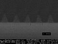
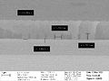
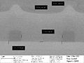
Etch rate uniformity tests on none patterned wafers

- Other tests with less good uniformity and lower etch rate
-
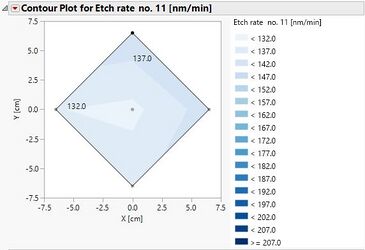 No. 11: Average etch rate: 135.7 nm/min +-3.7%
 -
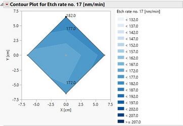 No. 17: Average etch rate: 174.5 nm/min +-4.2%
 -
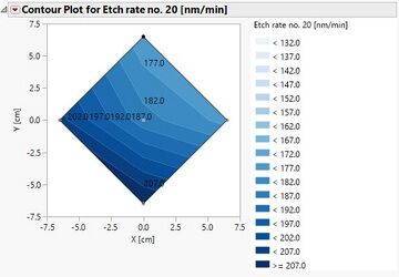 No. 20: Average etch rate: 189.8 nm/min +-10.5%


