Specific Process Knowledge/Etch/DRIE-Pegasus

Important: New rules (as of August 2011) for using the Pegasus
Until August 2011 processing at the Pegasus was complicated by frequent losses of wafers during transfer operations. It is evident that the instrument is much more susceptible to misalignments of the carousel than expected. A service engineer from SPTS has made a thorough realigning of the instrument that we hope will last a long time. We have therefore introduced a new set of rules that all users should be taught during a new training session mandatory for all users regardless of prior experience. The rules are:
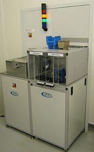
- All wafers must be processed using the MACS cassette loader. The only exceptions are bonded wafers and 150 mm wafers - see point 3. Batch recipes must be prepaired - even for single wafer trial runs.
- The backsides of the wafers must be absolutely clean: Wipe with IPA or blow dry the backside of every wafer.
- Loading bonded wafers (only bonded wafers and 6" wafers) using the load lock must be done with utmost care avoiding to change the position of the carousel.
- Processing using the MACS may be done either manually or automatically.
Please contact Roy, Peter or Jonas to make a training session.
The DRIE Pegasus at Danchip
The DRIE Pegasus is a state-of-art silicon dry etcher. It offers outstanding performance in terms of etch rate, uniformity etc. This page will provide some clues.
The Bosch process in the DRIE-Pegasus
This section introduces the advanced Bosch process used at the Pegasus and the process options it offers. Specific_Process_Knowledge/Etch/DRIE-Pegasus/System-description
The standard processes: Processes A, B, C, D and SOI
The instrument was accepted on the basis of the performance of 5 processes. These standard processes are described below.
| Process name | Type | Purpose | Conditions during original runs | Best usage | |||
|---|---|---|---|---|---|---|---|
| Feature | Mask material | Etch load | Comments | ||||
| Process A | Bosch | Fast etch | 80 µm trench | Photo resist | 12-13 % on 6" wafer | ||
| Process B | Bosch | Fast etch | 30 µm diameter via | Photo resist | 12-13 % on 6" wafer | ||
How to read the SPTS notation on process recipes
To understand the SPTS short hand notation on process recipes look at two examples from the etch cycle of step1 of the Process A described below:
- The Platen power has the setting 120 >> 140 (1.5s) 45 - it is to be interpreted as:
- In the first 1.5 seconds of the every cycle the platen power has a value that is ramped (indicated by >>) from 120 W initially to 150 W in the end
- During the remainder of the cycle the platen power is kept constant at 45 W.
- The Pressure has the setting 25 (1.5 s) 90 >> 150 - it is to be interpreted as:
- In the first 1.5 seconds the pressure is constant at 25 mtorr.
- During the remainder of the cycle the pressure has i higher value that is ramped from 90 initially to 150 mtorr in the last etch cycle.
Process A
Process A is labelled Large trench (80μm wide) 150μm depth. In the acceptance test the process was run on a 150 mm SPTS wafer with 12-13 % etch load.
Process A: Recipe, specifications and results
Process B
Process A is labelled Via (30μm diameter) 100μm depth. In the acceptance test the process was run on a 150 mm SPTS wafer with 12-13 % etch load.
Process B: Recipe, specifications and results
Process C
Process A is labelled Nano silicon etch. In the acceptance test the process was run on a 100 mm Danchip wafer with a test pattern of a series of lines and dots with sizes ranging from 30 nm to 300 nm. The etch load was extremely high, approaching 100 %.
Process C: Recipe, specifications and results
Process D
Process D is labelled Micro stamp etch.
In the acceptance test the process was run on a 100 mm wafer with 50 % etch load.
Process D: Recipe, specifications and results
SOI etch
The SOI etch uses the Low frequency (LF) platen generator to minimize the notching at buried stop layers such as the BOX layer in a SOI wafer.
SOI etch: Recipe, specifications and results
Other processes
Nanoetching
Wafer thinning
Sloped sidewalls
For injection molding purposes
Processing challenges
Bonded wafers
User manuals
- The Danchip user manual from LabManager is found >Here<.
- The user manual provided by SPTS can be found here >HERE<
Hardware information
Hardware Information - Overview.
Hardware Information - Detailed.
The Advantages the Pegasus has over existing Si etchers.
Robot Handling System Information .
Process applications
The acceptance test for the DRIE-Pegasus system, April 2010.
Further info:
