Old SIO2 etch recipe - unstable
SiO2 etch with resist mask on wafer with clamping and He backside cooling
Unless otherwise stated, all content in this section was done by Berit Herstrøm, DTU Nanolab, May 2018
The ASE is now the "dirty" plasma etcher at Nanolab meaning small amount of metals are allowed to be exposed by the plasma. That calls for recipes etching Silicon oxide and silicon nitride as well as silicon in this machine.
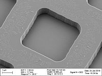
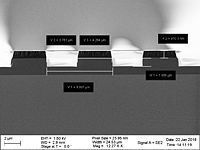
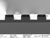
Not a lot experiments have been done yet etching SiO2 on wafers that are clamped and cooled but here is the best result so fare.
*This recipe is no longer stable.
| Parameter
|
SiO2 before etch
|
Resist before etch
|
Coil power
|
Platen power
|
Pressure
|
Flow rate C4F8
|
Flow rate H2
|
Flow rate He
|
T
|
Process time
|
Comment
|
Results
|
CD change
|
Profile angles
|
Etch rate in SiO2
|
Etch rate in resist
|
Selectivity (SiO2:resist)
|
Etch rate in Si and SiN
|
| 1SIOICP1
|
1892nm
|
1.4µm
|
800W
|
15 W
|
2.5mTorr
|
13sccm
|
26 sccm
|
|
20
|
15:00 min
|
Residues on the surface is coming when the resist is removed by plasma ashing, so remove the resist with 1165 remove and ultra sound to avoid this. 
|

|

|
.
|
63 nm/min
|
27 nm/min
|
2.3
|
bghe@Nanolab 2019-01-17
- Si:16-17 nm/min in the middle of the wafer (80% load)
- Si:14-15 nm/min at the edge of the wafer (80% load)
Emil Christian Stillhoff Jensen @Nanolab 2021-07-31
- SiN(700 nm PECVD nitrid): >46nm/min
|
SiO2 etch with resist mask on wafer with clamping and He backside cooling
Unless otherwise stated, all content in this section was done by Berit Herstrøm, DTU Nanolab, May 2018
The ASE is now the "dirty" plasma etcher at Nanolab meaning small amount of metals are allowed to be exposed by the plasma. That calls for recipes etching Silicon oxide and silicon nitride as well as silicon in this machine.
Not a lot experiments have been done yet etching SiO2 on wafers that are clamped and cooled but here is the best result so fare.
*This recipe is no longer stable.
| Parameter
|
SiO2 before etch
|
Resist before etch
|
Coil power
|
Platen power
|
Pressure
|
Flow rate C4F8
|
Flow rate H2
|
Flow rate He
|
T
|
Process time
|
Comment
|
Results
|
CD change
|
Profile angles
|
Etch rate in SiO2
|
Etch rate in resist
|
Selectivity (SiO2:resist)
|
Etch rate in Si and SiN
|
| 1SIOICP1
|
1892nm
|
1.4µm
|
800W
|
15 W
|
2.5mTorr
|
13sccm
|
26 sccm
|
|
20
|
15:00 min
|
Residues on the surface is coming when the resist is removed by plasma ashing, so remove the resist with 1165 remove and ultra sound to avoid this. 
|

|

|
.
|
63 nm/min
|
27 nm/min
|
2.3
|
bghe@Nanolab 2019-01-17
- Si:16-17 nm/min in the middle of the wafer (80% load)
- Si:14-15 nm/min at the edge of the wafer (80% load)
Emil Christian Stillhoff Jensen @Nanolab 2021-07-31
- SiN(700 nm PECVD nitrid): >46nm/min
|

