Specific Process Knowledge/Thin film deposition/ALD Picosun R200/TiO2 deposition using ALD
Feedback to this page: click here
The ALD window for titanium dioxide (TiO2) ranges from 120 oC to 350 oC.
A low temperatures between 120 oC and 150 oC an amorphous TiO2 layer is grown in the ALD, and at higher temperatures between 300 oC and 350 oC an anatase TiO2 layer is grown. At temperatures between 150 oC and 300 oC the TiO2 layer will be a mixture of both amorphous and anatase TiO2.
For Si wafers, amorphous TiO2 is best grown on wafers with native oxide, and anatase TiO2 is best grown on wafers without native oxide (removed using HF).
TiO2 standard recipe
Recipe: TiO2
Maximum deposition thickness: 100 nm
Temperature: 120 oC - 350 oC
| TiCl4 | H2O | |
|---|---|---|
| Nitrogen flow | 150 sccm | 200 sccm |
| Pulse time | 0.1 s | 0.1 s |
| Purge time | 4.0 s | 5.0 s |
TiO2 deposition rates and uniformity
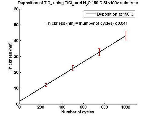
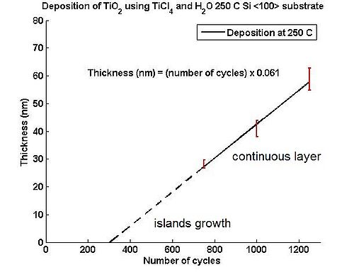
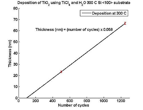
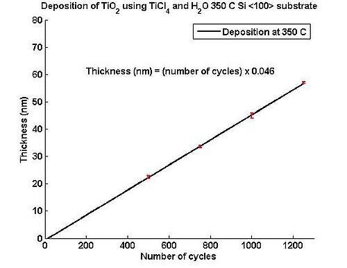
In the graphs below the TiO2 thickness as function of the number of cycles for deposition temperatures between 150 oC and 350 oC can be seen. Results have been obtained for <100> 100 mm Si wafers with native oxide or BHF treated wafers. The uniformity, thickness, refractive index has been obtained using Ellipsometer VASE.
- Titanium dioxide thickness as function of number of cycles
-
Temperature 150 oC Silicon wafer with native oxide.
-
Temperature 250 oC Silicon wafer with native oxide.
-
Temperature 300 oC Silicon wafer with BHF treated surface.
-
Temperature 350 oC Silicon wafer with BHF treated surface.
-
Temperature 150 oC Silicon wafer with native oxide. Amorphous TiO2 layer.
-
Temperature 350 oC Silicon wafer with BHF treated surface. Anatase polycrystalline layer.
Evgeniy Shkondin, DTU Danchip, 2014-2016.
TiO2 SEM results
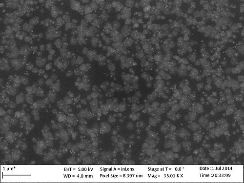
Some some SEM images reveals different surface morphology of TiO2 deposited on a Si surface at different temperatures between 150 oC and 350 oC are shown below. Some of samples have been treated with HF (hydrofluoric acid) to remove the native oxide layer just before the ALD deposition.
- Titanium dioxide deposited at different temperatures on a Si surface
-
Temperature 150 oC, 1200 cycles, HF treated Si surface.
-
Temperature 150 oC, 1200 cycles, Si surface with native oxide.
-
Temperature 250 oC, 750 cycles, Si surface with native oxide.
-
Temperature 300 oC, 1000 cycles, HF treated Si surface.
-
Temperature 300 oC, 1000 cycles, Si surface with native oxide.
-
Temperature 350 oC, 1250 cycles, HF treated Si surface.
Evgeniy Shkondin, DTU Danchip, 2014-2016.
TiO2 standard recipe characterization across 100 mm Si <100> wafer
| Deposition of amorphous and polycrystalline (anatase TiO2) | ||||||||||||||||||||||||||||||||||||||||||||||||||||||||||||||
|
| ||||||||||||||||||||||||||||||||||||||||||||||||||||||||||||||
Evgeniy Shkondin, DTU Danchip, 2014-2016.
TiO2 XPS investigation for elemental trace analysis
XPS profile for TiO2 has been obtained using XPS-ThermoScientific.
Typical profile for TiO2
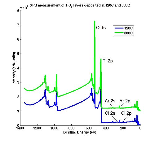
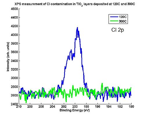
XPS measurements of TiO2 deposited at 120 oC and 300 oC are shown below. From the XPS measurements it can be calculated that at temperatures below 120 oC the TiO2 layer will be contaminated with about 1-3 % chlorine molecules from the TiCl4 precursor.
- Titanium dioxide deposited at different temperatures on a Si surface
-
Survey scan. Temperatures 120 oC and 300 oC, 500 cycles.
-
Measurement of the major contamination (Cl). Temperatures 120 oC and 300 oC, 500 cycles.Raising temperature to 300 oC reduces Cl contamination below the detectable level.
Evgeniy Shkondin, DTU Danchip, 2014-2016.
TiO2 deposition on trenches
Recipe: TiO2T
Maximum deposition thickness: 100 nm
Temperature: 120 oC - 350 oC
| TiCl4 | TiCl4 | H2O | H2O | |
|---|---|---|---|---|
| Nitrogen flow | 150 sccm | 150 sccm | 200 sccm | 200 sccm |
| Pulse time | 0.1 s | 0.1 s | 0.1 s | 0.1 s |
| Purge time | 0.5 s | 20.0 s | 0.5 s | 20.0 s |
A special recipe called "TiO2T" has been developed for the high aspect ratio structures. Is this recipe each precursors is introduced into the chamber in two steps, first followed by a very short purge time and then followed by a longer purge time.The recipe is good for deposition on very high aspect ratio structures (with aspect ratio more then 1:20) such as deep narrow trenches, pillars, pores etc. However, in most cases, including deposition on black silicon or other lower aspect ratio structures, the standard TiO2 recipe is sufficient and should be used instead! TiO2T can also be used for deposition on polymers at low temperatures (80-120 oC).
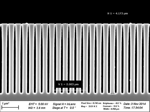
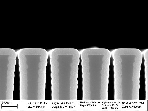
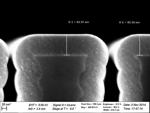
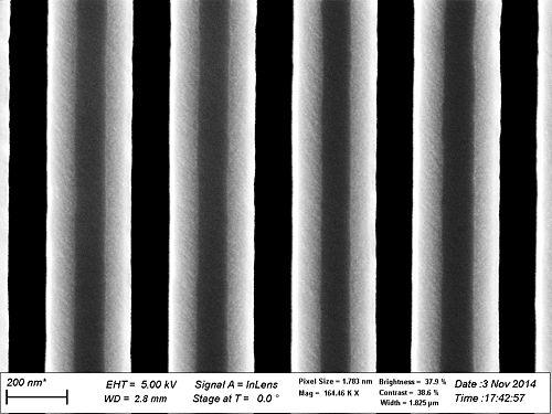
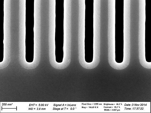
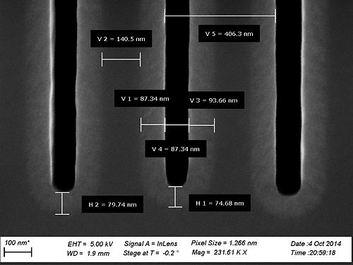
Below some SEM images of amorphous TiO2 deposited at 150 oC on Si trenches are shown. The width of the trenches is 200 nm, and the depth is 4 µm, i.e. the aspect ratio is 1:20. The number of cycles is 2000, and this results in a TiO2 layer of about 90 nm. The purge times corresponds to the ones shown in the table above. From the SEM images it is seen that the TiO2 layer covers the trenches very well. Trenches prepered using (DRIE-Pegasus). Research results based on this recipe can be found here: LINK
- Amorphous titanium dioxide deposited on Si trenches
- Anastase titanium dioxide deposited on Si trenches
Evgeniy Shkondin, DTU Danchip, 2014-2016.

