Specific Process Knowledge/Etch/DRIE-Pegasus/processA
Feedback to this page: click here
Process A
Process A is labelled Large trench (80μm wide) 150μm depth. In the acceptance test the process was run on a 150 mm SPTS wafer with 12-13 % etch load.
| Parameter | Specification | Average result |
|---|---|---|
| Etch rate (µm/min) | > 15 | 18.9 |
| Etched depth (µm) | 150 | 189.1 |
| Scallop size (nm) | < 800 | 718 |
| Profile (degs) | 91 +/- 1 | 91.1 |
| Selectivity to AZ photoresist | > 150 | 310 |
| Undercut (µm) | <1.5 | 0.84 |
| Uniformity (%) | < 3.5 | 3.0 |
| Repeatability (%) | <4 | 0.43 |
The process developed by SPTS that fulfilled these criteria had the following parameters:
| Step 1 | Step 2 | |||
|---|---|---|---|---|
| Parameter | Etch | Dep | Etch | Dep |
| Gas flow (sccm) | SF6 350 (1.5 s) 550 | C4F8 200 | SF6 350 (1.5 s) 550 | C4F8 200 |
| Cycle time (secs) | 7.0 | 4.0 | 7.0 | 4.0 |
| Pressure (mtorr) | 25 (1.5 s) 90 >> 150 | 25 | 25 (1.5 s) 150 | 25 |
| Coil power (W) | 2800 | 2000 | 2800 | 2000 |
| Platen power (W) | 120 >> 140 (1.5) 45 | 0 | 140 (1.5) 45 | 0 |
| Cycles | 11 (keep fixed) | 44 (vary this) | ||
| Common | Temperature 20 degs, HBC 10 torr, Short funnel, with baffle & 5mm spacers | |||
QC template - try to make you QC recipe + limits look as much as possible like this
| Quality Controle (QC) for RIE1 and RIE2 | |||||||||||||||||||||||
|
Process A guidelines
Process A is optimized for speed and depending on feature size and etch load it will achieve etch rates up to 25-30 µm/min.
This aggressive etch has a few drawbacks - one of which is the release of energy in the etch process. In general, it is clear that
- The higher the etch rate, the higher rate of released energy.
- The larger an area of silicon is exposed to plasma and hence etched, the higher rate of released energy.
Given its high etch rate, Process A is very sensible to high etch load processes and substrates with reduced cooling efficiency. Therefore, users are generally advised to
- Use Process A with precaution at high etch loads - above some 50%.
- Avoid using Process A on bonded wafers, in particular if the etch load is more than 5-10%. The bonding reduces the heat conduction across the wafer interface so the top wafer will immediately heat up and cause the mask to erode and the bonding polymer to melt.
If you have a bonded sandwich of wafers with very poor heat conduction (typically caused by intermediate polymer layers thicker than a few microns) you are advised to use other etch processes, maybe the deepetch on the ASE.
Process A performance
The perfomance of Process A has been investigated as a function of feature size and etch load.
Experiment
A number of wafers are patterned with the travka masks in AZ photoresist or 600 nm oxide. The wafers are then etched (batch recipe with 5 minute TDESC interstep cleans) using two different durations of process A in the DRIE-Pegasus.
|
|
Results: Optical images
- Optical images of the C01548 batch that is processed 10:05 mins.
-
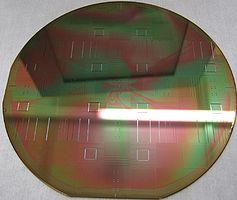 Wafer C01548.01: 5 % exposed area
 -
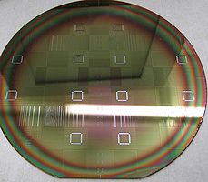 Wafer C01548.02: 10 % exposed area
 -
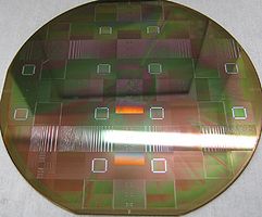 Wafer C01548.03: 20 % exposed area
 -
 Wafer C01548.04: 35 % exposed area
 -
 Wafer C01548.05: 50 % exposed area


- Optical images of the C01549 batch that is processed 20:10 mins.
-
 Wafer C01549.01: 5 % exposed area. Some 190 nm of 600 nm oxide remains.
 -
 Wafer C01549.02: 10 % exposed area. Some 122 nm oxide remains.
 -
 Wafer C01549.03: 20 % exposed area. In the centre some 90 nm oxide remains.
 -
 Wafer C01549.04: 35 % exposed area. In the centre some 90 nm oxide remains.
 -
 Wafer C01549.05: 35 % exposed area (close-up). The oxide has disappeared leaving the Si exposed.


The etching of silicon releases energy. This means that the faster the etch is, the more heat needs to be dissipated. The consequence is the same if a larger percentage of the wafer is etched. Process A is the fastest etch and as seen above, the exposed area plays an important role. As the exposed area increases the oxide mask erosion is more and more pronounced.
If a larger area is to be etched, the cooling must be made more efficient, either by lowering the platen temperature or with increasing the pressure of He on the backside of the wafer. This will be investigated soon.
Results: Etched depths in trenches of different widths
- Graphs
-
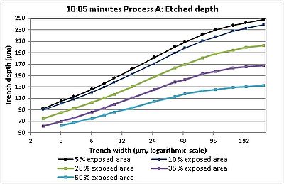 Process time 10:05
 -
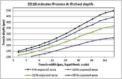 Process time 20:10

