Specific Process Knowledge/Thermal Process/RTP Jipelec 2
Feedback to this page: click here
RTP Jipelec 2 - Rapid Thermal Processer/Annealer

January 2021: The RTP Jipelec 2 is not released for use yet
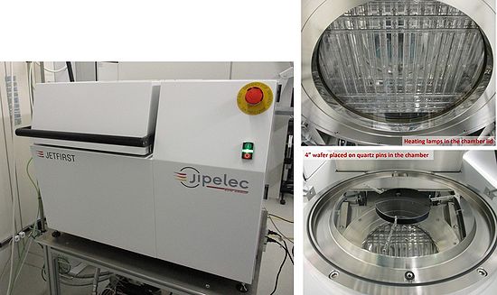
Jipelec JetFIRST 200 RTP (Rapid Thermal Processer/Annealer).
The main purpose of the machine is to anneal different samples very rapidly. Furthermore, the machine can be used for alloying of different materials.
The annealing is done in a process chamber on the machine, in which the samples are heated very rapidly by use of infra red lamps placed in the top of the chamber, directly above the sample(s). The chamber walls are cooled and remains cold during the annealing.
Samples can be wafers (2". 4", 6" and 8") or smaller samples made of different materials. In the process chamber, the samples are placed on quartz pins, either directly on the pins (only wafers) or on a graphite sucseptor or a Si dummy wafer.
The maximum annealing temperature is 1200 C. For temperatures above 700 C the annealing time is limited as can be seen in the table below.
The temperature is measured by either a thermocouple or an optical pyrometer. The temperature is regulated by a PID controller, thus the PID values will have to be optimized for each susceptor size and for each wafer size and thickness, and it is important to select the right PID table for each process.
Annealings can be done at atmospheric pressure or in vacuum. It is also possible to apply a flow of either nitrogen or argon during the annealing, and forming gas (4 % H2/96 % N2) will be connected later.
The user manual, user APV, technical information and contact information can be found in LabManager:
| Purpose | Rapid thermal processor/annealer | |
|---|---|---|
| Process parameter range | Process temperature |
Annealing temperature:
Temperature ramp:
|
| Process pressure |
| |
| Gases on the system |
Process gases:
Purge gas:
| |
| Substrates | Batch size |
|
| Substrate materials allowed |
A carrier is always needed: For III-V materials a carbide carrier is used, and for other samples a silicon carrier wafer with 1 µm oxide is used
|
