Specific Process Knowledge/Thin film deposition/Cluster-based multi-chamber high vacuum sputtering deposition system
Feedback to this page: click here

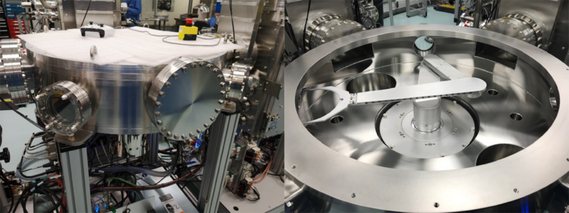
Cluster-based multi-chamber high vacuum sputtering deposition system is a robotic cluster tool with two deposition chambers sharing the same distribution trasfer station and the load-lock. The equipment has been installed and accepted in clean-room during January 2020. The purpose of the tool is to deposite variety of materials using DC/RF/PulseDC/HIPIMS magnetron sputtering with or without RF substrate bias. In modul A or PC 1 (process chamber 1) it is possible to deposit any materials using 6 x 3” magnetrons sourses with N2 or O2 reactive gases. Modul B or PC 3 (process chamber 3) is dedicated to oxygen free materials - nitrides and metals. It is eqipted with 1 x 4” + 2 x 3” magnetrons and supplied with N2 process gas for reactive deposition. Both chambers allow heating of substrates up to 600 oC. The equipment is located in clean-room A-5 where the user can acces the cassete loader.
Manufacture: Kurt J. Lesker Company
Model: 2017 PRO Line PVD75 thin film deposition cluster system
The user manual, user APV and contact information can be found in LabManager:
Sputter-System Metal-Oxide(PC1)
Sputter-System Metal-Nitride(PC3)
Thin Film group thinfilm@nanolab.dtu.dk is responsible of the equipment
Target/Metal requests should be sent to metal@nanolab.dtu.dk
If you need a training on the machine please send your request to: training@nanolab.dtu.dk.
Sputtering deposition system set-up
In the graphs below the HfO2 thickness vs. number of cycles for deposition temperatures between 150 oC and 350 oC presented. Results have been obtained for <100> 150 mm Si wafers with native oxide, based on ellipsometry study.
- System set-up and power supply configuration.
-
 Deposition rate of HfO2 at 150 oC. Substrate: Silicon 6" wafer with native oxide.

Power suppliy configuration
Power supplies specification presented in a table below.
| Power Supply ID | Type | Maximum output power (W) | Maximum output voltage (V) | Maximum output current (A) | Comments
|
|---|---|---|---|---|---|
| PC1 Power Supply 1 | RF | 300 | |||
| PC1 Power Supply 3 | DC | 500 | 1000 | 4 | |
| PC1 Power Supply 4 | DC | 500 | 1000 | 4 | |
| PC1 Power Supply 5 | Pulse DC | 2000 | 800 | 5 |
Max frequency: 100kHz |
| PC1 Power Supply 7 | RF (Substrate) | 100 | |||
| PC3 Power Supply 1 | RF | 300 | |||
| PC3 Power Supply 2 | Pulse DC | 2000 | 800 | 5 |
Max frequency: 100kHz |
| PC3 Power Supply 3 | DC to HiPIMS | 1500 | 1000 | 4 |
HiPIMS Unit
|
| PC3 Power Supply 5 | DC | 500 | 1000 | 4 |
|
| PC3 Power Supply 6 | RF (substrate) | 100 |
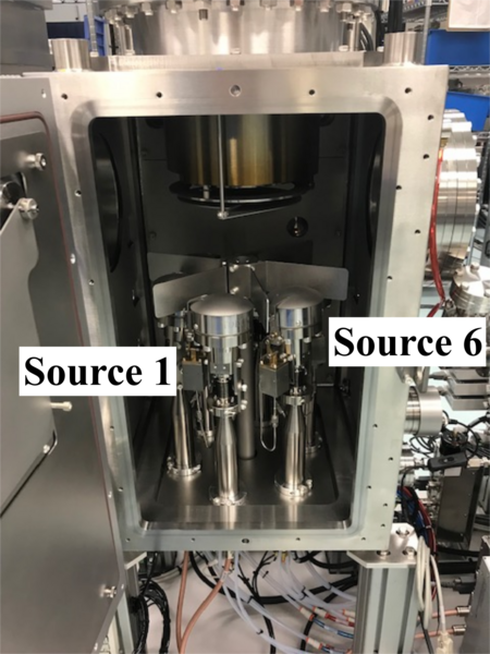
Sputter-System Metal-Oxide (PC1)
Chamber PC1 consists of six KJLC Torus® 3" magnetron sputtering sources with possibility of RF, DC, Pulse DC and HIPIMS sputtering. There are Argon, Nitrogen and Oxygen gas lines connected to this chamber.
- Process chamber (PC 1)
-
 Photography of the chamber.
 -
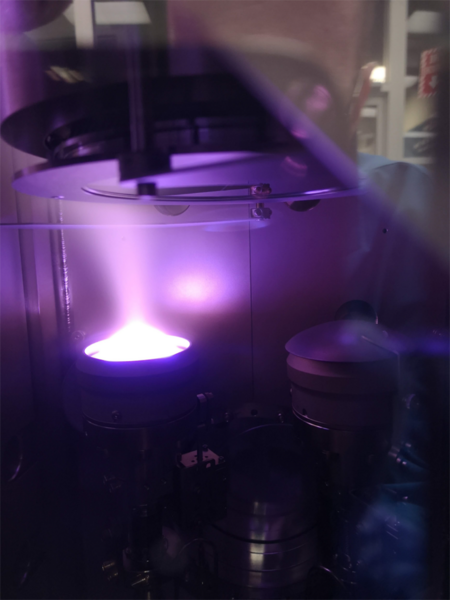
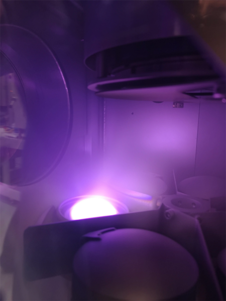 Deposition from source 2.


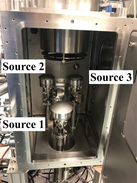
Sputter-System Metal-Nitride (PC3)
The second process chamber called PC3 consists of two KJLC Torus® 3" magnetron sputtering sources and one height adjustable KJLC Torus® 4" magnetron sputtering source, also with possibility of RF, DC, Pulse DC and HIPIMS sputtering. The chamber has a possibility to do the RF bias on a substrate, which can be used as substrate cleaning before the deposition or used during the deposition to alter the film properties.
- Deposition rates of HfO2 at different temperaturs. ALD window.
-
 Deposition rate of HfO2 at 150 oC. Substrate: Silicon 6" wafer with native oxide.
 -
 Deposition rate of HfO2 at 150 oC. Substrate: Silicon 6" wafer with native oxide.


Distribution Chamber (Genmark robot)
bla bla
- Deposition rates of HfO2 at different temperaturs. ALD window.
-
 Deposition rate of HfO2 at 150 oC. Substrate: Silicon 6" wafer with native oxide.

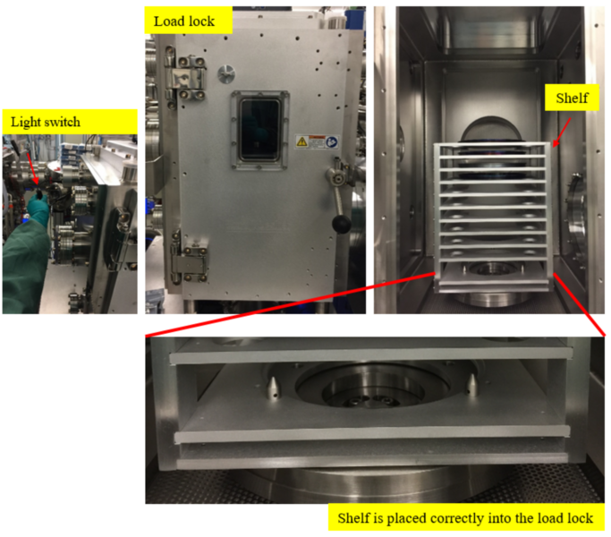
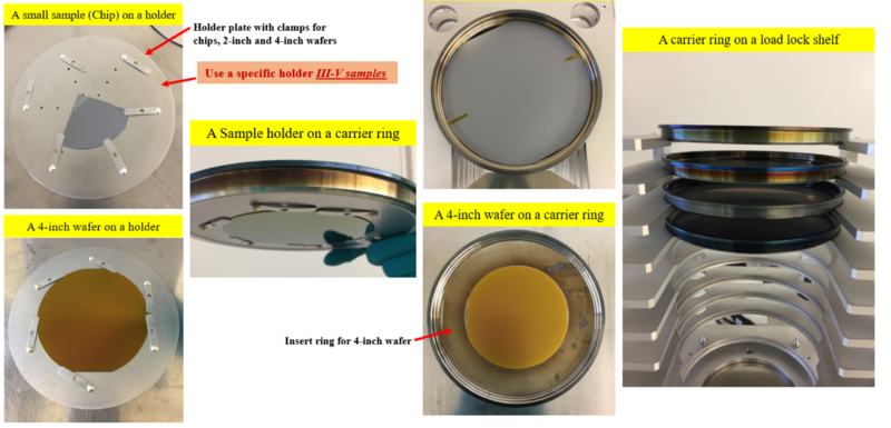
Load lock
bla bla bla bla
Bla bla
- Deposition rates of HfO2 at different temperaturs. ALD window.
-
 Deposition rate of HfO2 at 150 oC. Substrate: Silicon 6" wafer with native oxide.
 -
 Deposition rate of HfO2 at 150 oC. Substrate: Silicon 6" wafer with native oxide.


Process information
Too high sputter power can cause target or sputter gun damage. Given the target/interface thermal limitations, such damage can be reduced/eliminated by using an appropriate maximum power. However, "appropriate" often equates to "low" and low power means low deposition rate. Once the appropriate power has been established for a given target/gun, never switch on and immediate increase power to that value! Always increase power slowly to its maximum value through a series of ramps. When the deposition run is complete, it is equally important to ramp down power at the same rate at ramp up, allowing the target to cool slowly to avoid thermal shock and the potential for target fracture.
| Target size | Target material | Maximum Power density (W/inch2) | Maximum Power (W) | Maximum Ramp up/down Power (W/s) | Comments
|
|---|---|---|---|---|---|
| 3 inch | Al | 150 | 1000 | 10 | DC/HiPIMS |
| Au | 100 | 700 | 10 | DC/HiPIMS | |
| Ag | 100 | 700 | 10 | DC/HiPIMS | |
| Cu | 200 | 1400 | 10 | DC/HiPIMS | |
| Ni | 50 | 350 | 10 | High strengh magnets/DC | |
| Ti | 50 | 350 | 10 | DC/HiPIMS | |
| Ge (Bonded) | 20 | 140 | 0.3 | DC/RF | |
| Si (Unbonded/Bonded) | 20 | 140 | 0.3 | RF
| |
| SiO2 (Bonded) | 20 | 140 | 0.3 | RF
| |
| ITO (Bonded) | 20 | 140 | 0.3 | RF/PDC
| |
| BaTiO3 (Bonded) | 20 | 140 | 0.3 | RF
| |
| NbTi | 50 | 350 | 10 | DC | |
| 4 inch | Al | 150 | 1800 | 10 | DC/HiPIMS |
Standard recipe performance
There are in total 76 developed and tested process recipes for general users (48 for PC1 and 28 for PC3). Starting the recipe the user can change te relevant process parameters: power, pressure, reactive gas ratio, rotation speed, substrate bias etc. In addition to the process recipes, there are also recipes for substrate heating and RF cleaning.
Bla bla
- Deposition rates of HfO2 at different temperaturs. ALD window.
-
 Deposition rate of HfO2 at 150 oC. Substrate: Silicon 6" wafer with native oxide.

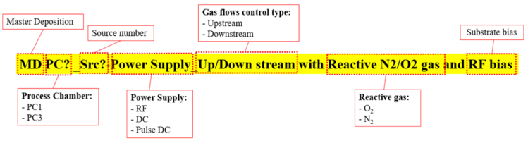
| Recipe name | Target material | Pressure (mTorr) | Power (W) | Deposition rate (nm/min) | Uniformity (%) on 6 inch wafer |
Comments
|
|---|---|---|---|---|---|---|
| MD PC1 Src1 RF Upstream | SiO2 | 3 | 140 (RF) | 2.3 | 0.5 | |
| MD PC1 Src2 RF Upstream | SiO2 | 3 | 140 (RF) | 2.6 | 3 | |
| MD PC1 Src3 DC Upstream | Ni | 3 | 500 (DC) | 23.3 | 2.5 | |
| MD PC1 Src4 DC Upstream | Cu | 3 | 500 (DC) | 52.2 | 2.2 | |
| MD PC1 Src5 DC Upstream | Al | 3 | 200 (DC) | 7.9 | 3.2 | |
| MD PC1 Src5 Pulse DC Downstream with reactive O2 |
Al | 3 | 500 (PDC) Frequency: 100Hz Reverse time: 2µs |
1.7 | 3.4 | Ar flow: 50sccm O2 flow: 15 sccm
|
| MD PC1 Src6 Pulse DC Upstream | ITO | 3 | 140 (PDC) Frequency: 100Hz Reverse time: 2µs |
11 | 4.5 | |
| MD PC1 Src6 Pulse DC Downstream with reactive O2 |
ITO | 3 | 140 (PDC) Frequency: 100Hz Reverse time: 2µs |
11.3 | - | Ar flow: 50sccm O2 flow: 2 sccm |
| MD PC1 Src1 RF Upstream | Si | 3 | 120 (RF) | 1.8 | - | |
| MD PC3 Src1 Pulse DC Downstream with reactive N2 |
Al | 3 | 900 (PDC) Frequency: 100Hz Reverse time: 2µs |
29 | 3.2 | Ar flow: 50sccm O2 flow: 15 sccm |