Specific Process Knowledge/Thin film deposition/Furnace LPCVD TEOS
Ikke skevet!
LPCVD (Low Pressure Chemical Vapor Deposition) TEOS

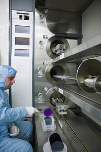
At the moment there is one furnace for TEOS oxide depositions at Danchip. The furnace is a Tempress horizontal furnace. The process is a batch process meaning you can run a batch of 10 wafers at a time. The deposition takes place at temperatures of 725 degrees Celsius. The reactive gases are dinitrogenoxide and silane. The LPCVD TEOS has a excellent step coverage and extreamly good for trench filling and the film thickness is very uniform over the wafer. We have two standard LPCVD TEOS processes: One that opens slowly for depositing thick layers (>750nm) and one for deposition of thin layers that opens faster. To get information on how to operate the furnace please read the manual which is uploaded to LabManager. Remember to anneal the TEOS oxide to improve the electrical properties as well as chemical resistance.
Process Knowledge
Please take a look at the process side for deposition of TEOS oxide:
Deposition of Silicon Nitride using LPCVD
| Purpose | Deposition of TEOS silicon oxide |
|
|---|---|---|
| Performance | Film thickness| |
|
| Step coverage |
| |
| Film quality |
| |
| Process parameter range | Process Temperature |
|
| Process pressure |
| |
| Gas flows |
| |
| Substrates | Batch size |
|
| Substrate material allowed |
|
