Specific Process Knowledge/Characterization/AFM: Atomic Force Microscopy/AFM Icon Acceptance
Feedback to this page: click here
AFM Icon 1 accessories and acceptance test
Accessories following the system 
| Equipment | AFM Icon | AFM Icon 2 |
|---|---|---|
| Chucks |
|
|
| Holders |
|
|
| Modes included |
|
|
| Up to 13µm | Up to 13µm | |
| <30pm RMS | <30pm RMS | |
| <0.15nm RMS | <0.15nm RMS | |
| 35pm RMS | 35pm RMS | |
| <0.5% | <0.5% | |
| <0.15nm RMS | <0.15nm RMS | |
| ~1 for our standard probe. Can be improved to about 10 with the right probe | ~1 for our standard probe. Can be improved to about 10 with the right probe | |
| Hardware settings | Standard probe: <12 nm | Standard probe: <12 nm |
| ScanAsyst in Air | ScanAsyst in Air | |
| Tap300Al-G | Tap300Al-G | |
| SSS-NCHR | ||
| AR5-NCHR | AR5-NCHR | |
| Substrates | Up to 210mm in diameter and up to 15mm thick" | Up to 210mm in diameter and up to 15mm thick" |
|
| |
| In principle all materials | In principle all materials |
Extra chuck
We have two chucks:
- A symmetric chuck that handles up to 210mm wafers and 15mm thick
- An asymmetric chuck that handles up to ~4" wafer (but not small pieces) - using this a whole 4" can be accessed without rotating the sample.
Holders
- Magnetic sample holder + magnetic discs + double sided tape
- Holder for vertical profile scans
Modes included
- ScanAsyst
- TappingMode (air)
- Contact Mode
- Lateral Force Microscopy
- PhaseImaging
- Lift mode
- MFM
- Force Spectroscopy
- Force volume
- EFM
- surface potential
- Torsional Resonance Mode
- Piezoresponse Microscopy
- Force spectroscopy
Extra modes:
- PeakForce KPFM package (incl extra box for high voltage PF KPFM)
- PFQNM package
- Microscope Image Registration and Overlay (MIRO) software. this is only working in the old software (before version 9.4)
Probes
Probes that followed the system (we may not have them anymore!)
| ScanAsyst mode | Tapping mode | Contact mode | PF-KPFM | |
|---|---|---|---|---|
| Generel description | Generel description | Generel description | ||
| Probes that followed the system |
|
|
|
|
Samples
- QC grid: VGRP-15M 10µm pitch and depth reference 178nm
- PF KPFM-SMPL Kelvin probe Sample: Al + Au on Si
Calibration samples for getting quantitative modulus measurements:
- PDMS-soft-1-12M: PDMS gel 2.5MPa
- PDMS-soft-2-12M: PDMS gel 3.5MPa
- PSFilm-12M: Polystyrene filem
- FSilica-12M: Fused Silica
- Sapphire-12M: Sapphire
- RS-12M: Ti roughness sample
- HOPG-12M: Highly Orientated Pyrolytic Graphite
- PS-LDPE: Harmonix training
- HOPG: Highly Oriented Pyrolytic Graphite
Acceptance tests done
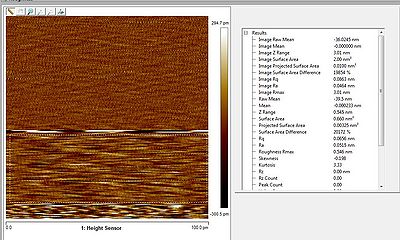
Noise tests
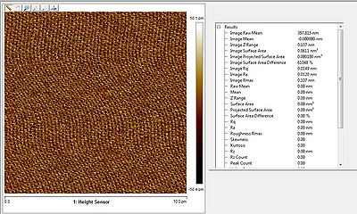
Sensor noise
Tappingmode, OTESPA-R3 probe used.
First we made a false engage (scanning in air):
Turn off gain 0 0
Z range 0.2my
Scan size 0.01nm
We saw some 50Hz noise (electrical - or maybe pumps): Rq 15 pm (specs 35pm)
System noise
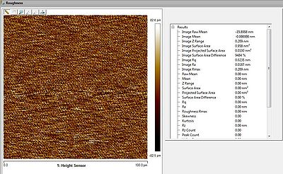
Noise on sample: scan size 0.1nm
we started with 1my scan size to optimize the scan.
2.43Hz
256 lines
Z range at 2my to get sub nanometer resolution in Z
Rq: 54,5pm (plade vibrator koerte udenfor)
Rq: 23pm uden vibrator koerende + ro og med aaben hood.
Rq:71pm uden vibrator koerende + ro og med lukket hood
Roughness
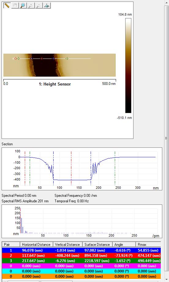
HAR: 200nm wide 400nm deep
HAR: 2µm wide 6µm deep
Graphene KPFM measurement
![]()
![]()
Height image: The graphene and structuring in graphene is not visible
Potential image: Potential difference between grapheme and non-graphene is visible
Phase: Phase imaging maps the phase lag between the periodic signal driving the cantilever and the oscillations of the cantilever. Changes in phase lag often indicate changes in the properties of the sample surface. Here the structuring in the graphene is very clear

