Specific Process Knowledge/Characterization/AFM: Atomic Force Microscopy/AFM Icon Acceptance
Feedback to this page: click here
This page has been made by Berit Herstrøm @ DTU Nanolab
Accessories following the systems
| Equipment | AFM Icon | AFM Icon 2 | ||||||||||||||
|---|---|---|---|---|---|---|---|---|---|---|---|---|---|---|---|---|
| Chucks |
|
| ||||||||||||||
| Holders |
|
| ||||||||||||||
| Modes included |
|
| ||||||||||||||
| Probes that followed the systems |
|
| ||||||||||||||
| Samples |
Calibration samples for getting quantitative modulus measurements:
|
|
AFM Icon-Pt 1: Acceptance tests done
Noise tests
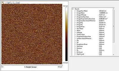
Sensor noise
Tappingmode, OTESPA-R3 probe used.
First we made a false engage (scanning in air):
Turn off gain 0 0
Z range 0.2my
Scan size 0.01nm
We saw some 50Hz noise (electrical - or maybe pumps): Rq 15 pm (specs 35pm)
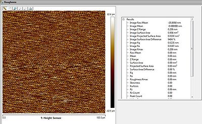
System noise
Noise on sample: scan size 0.1nm
we started with 1my scan size to optimize the scan.
2.43Hz
256 lines
Z range at 2my to get sub nanometer resolution in Z
Rq: 54,5pm (plade vibrator koerte udenfor)
Rq: 23pm uden vibrator koerende + ro og med aaben hood.
Rq:71pm uden vibrator koerende + ro og med lukket hood
Roughness
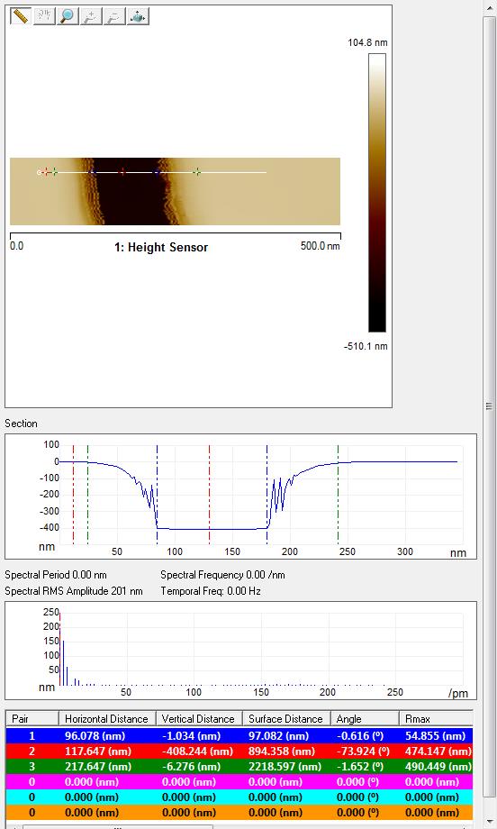
HAR: 200nm wide 400nm deep
HAR: 2µm wide 6µm deep
Graphene KPFM measurement
![]()
![]()
Height image: The graphene and structuring in graphene is not visible
Potential image: Potential difference between grapheme and non-graphene is visible
Phase: Phase imaging maps the phase lag between the periodic signal driving the cantilever and the oscillations of the cantilever. Changes in phase lag often indicate changes in the properties of the sample surface. Here the structuring in the graphene is very clear
AFM Icon-Pt 2: Acceptance test
Noise tests
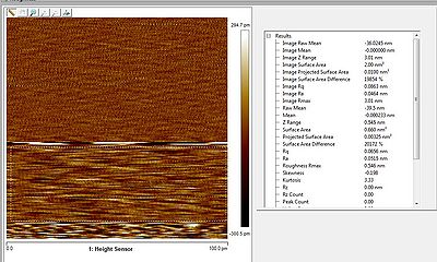
Sensor noise
Tapping ]mode, OTESPA-R3 probe used.
First we made a false engage (scanning in air):
Turn off gain 0 0
Z range 0.2my
Scan size 0.01nm
Roughness: Rq 28 pm (specs 35pm)
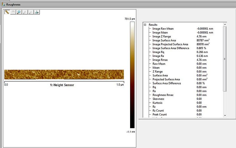
System noise
Noise on sample: scan size 0.1nm
we started with 1my scan size to optimize the scan.
2.43Hz
256 lines
Z range at 2my to get sub nanometer resolution in Z
Rq: 28 pm
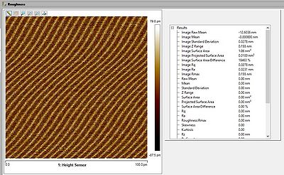
Demonstrating roughness measurements on silicon
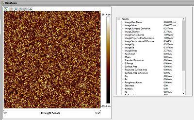
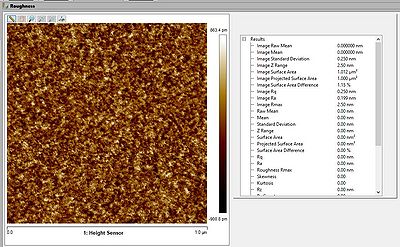
ScanAsyst with ScanAsyst-air
- CL on
- 512x512
- 0dg
- ScanAsyst noise threshold: 1
- PeakForce amplitide 300 nm
- Peak force frequency: 2 Hz
- Rq: 0.247 nm
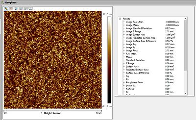
ScanAsyst with ScanAsyst-air
- CL off
- 512x512
- 0dg
- ScanAsyst noise threshold: 0.2
- PeakForce amplitide 300 nm
- Peak force frequency: 2 Hz
- Rq: 0.235 nm
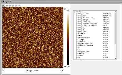
ScanAsyst with TAP150A
- CL on
- 512x512
- 0dg
- ScanAsyst noise threshold: 1
- PeakForce amplitude 75 nm (was set as standard from the probe settings)
- Peak force frequency: 2 Hz
- Rq: 0.238/0.250 nm
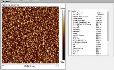
Tapping mode with TAP150A
- CL on
- 512x512
- 0dg
- Rq: 0.214 nm
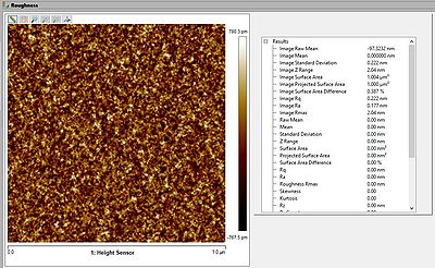
Tapping mode with RFESP-75
- CL on
- 512x512
- 0dg
- Rq: 0.224 nm
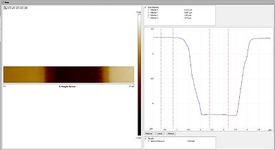
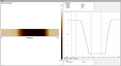
Step measurement: Resist on silicon oxide
SIO2ICP_30 (Si-SiO2-Resist)
- When scanning long lines and trenches scan 90 degrees to the probe and 90 degrees to the lines.
- During acceptance:
- Tapping mode: 3 µm structures (middle): 1.587µm
- Tapping mode: 3µm structures (edge): 1.541µm
- Peak Force tapping 3µm structures (edge) average: 1.497µm (tapping mode probe)
- Peak Force tapping with ScanAsyst probe: 1.509µm
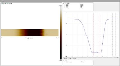
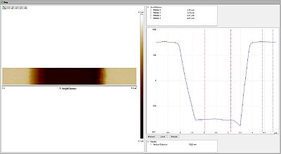
SEM images showed about 1.55µm – so it seems like ScanAsyst is pressing a little down in the resist compared with the SiO2 giving a too small height difference. Therefor When scanning steps with difference materials, when one of the materials is soft and you need to know the height difference, then it seems to be best to use tapping mode. We did not save the images. Therefor I remeasured a few days later:
Tapping mode with TAP150A
- CL on
- 256x32
- 0dg
- Step height: 1545/1532 nm
ScanAsyst with TAP150A
- CL on
- 256x32
- 0dg
- ScanAsyst noise threshold: 1
- PeakForce amplitide 75 nm (was set as standard from the probe settings)
- Peak force frequency: 2 Hz
- Step height: 1537 nm
ScanAsyst with ScanAsyst-air
- CL on
- 256x32
- 0dg
- ScanAsyst noise threshold: 1
- PeakForce amplitide 150 nm (I had to increase it from the 75 nm)
- Peak force frequency: 2 Hz
- Step height: 1545 nm
Tapping mode with RFESP-75
- CL on
- 256*32
- 0dg
- Step height: 1525 nm
High Aspect ratio sample
High aspect ratio samples (e.g. 100 nm wide trenches 300 nm deep and 2 µm wide trenches 6µm deep). The probes for this: FIB6-400A. This was done and work spaces were created but no images was saved.
