Specific Process Knowledge/Thin film deposition/thermalevaporator
THIS PAGE IS UNDER CONSTRUCTION
Feedback to this page: click here
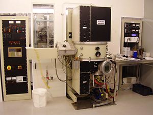
Alcatel - A system for deposition of metals

The user manual, quality control procedure and results, user APV, technical information and contact information can be found in LabManager:
Process information
Materials for e-beam evaporation
- Aluminium (Al)
- Chromium (Cr)
- Copper (Cu)
- Gold (Au)
- Molybdenum (Mo)
- Nickel (Ni)
- Palladium (Pd)
- Platinum (Pt)
- Silver (Ag)
- Tantalum (Ta)
- Tin (Sn)
- Titanium (Ti)
- Tungsten (W) - thinner layers
| Purpose | Deposition of metals and silicon |
|
|---|---|---|
| Performance | Film thickness |
|
| Deposition rate |
| |
| Process parameter range | Process Temperature |
|
| Process pressure |
| |
| Substrates | Batch size |
|
| Substrate material allowed |
| |
| Material allowed on the substrate |
|
* For thicknesses above 200 nm permission is requested.
