Specific Process Knowledge/Characterization/Profiler
{{cc-nanolab}
Feedback to this page: click here
DektakXTA info copied to https://labadviser.nanolab.dtu.dk//index.php?title=Specific_Process_Knowledge/Characterization/Dektak_XTA#Performance_and_Process_Parameters
P17 info copied to https://labadviser.nanolab.dtu.dk//index.php?title=Specific_Process_Knowledge/Characterization/Tencor_P17#Tencor_P17_Stylus_Profiler
info moved to https://labadviser.nanolab.dtu.dk//index.php?title=Specific_Process_Knowledge/Characterization/Sensofar_S_Neox
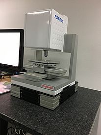
Optical Profiler (Filmetrics)
Unless otherwise stated, all content in this section was done by Berit Herstrøm, DTU Nanolab

The Profilm3D optical profiler from Filmetrics uses white-light-interferometry (WLI) and phase-shifting-interferometry (PSI) to produce surface profiles and depth-of-field color images.
The main purpose is 3D topographic imaging of surfaces, step height measurements and roughness measurements with larger FOV (Field Of View) than the AFM, but less horisontal resolution.
For most samples the optical profiler provides fast and easy information without any sample preparation. However, it can be necessary to cover thin transparent layers (< 2 µm) with a thin layer of metal.
The resolution is limited by the objective and the sampling resolution.
The user manual, technical information and contact information can be found in LabManager (requires login):
Optical profiler (Filmetrics) info page in LabManager
| Equipment | Optical profiler | |
|---|---|---|
| Purpose | 3D topographic imaging of surfaces. |
|
| Posibilities | Interferometric profiling |
|
| Performance | With the current 10x objective |
See here the data sheet for this instrument (requires login)] |
| Substrates | Substrate size |
|
| Substrate materials allowed |
| |
Dektak 3ST

The Dektak 3ST is intended for profile measurements on samples outside the cleanroom. It is located in the basement, building 346, room 904.
The user manual, technical information and contact information can be found in LabManager:
Dektak 3ST (Dektak) in LabManager
The computer connected to the Dektak 3ST is pretty old and runs Windows 98 SE. It is not connected to the network but traces can be saved on either USB memory stick or floppy disk. The USB driver is an old universal driver and has been shown to work with small size USB sticks. However it did not work with an 8GB Kingston stick.
| Performance | Vertical Range |
|
|---|---|---|
| Scan length range |
| |
| Stylus track force |
| |
| Scan speed ranges |
| |
| Materials | Allowed substrate materials |
|
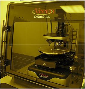
Stylus Profiler: Dektak150

The stylus profiler Dektak150 is intended for profile measurements on samples outside the cleanroom. The Dektak150 is especially well suited for measuring soft samples as it can be adjusted to apply lower force than the other stylus profilers at Nanolab.
The user manual, technical information and contact information can be found in LabManager:
Stylus profiler:Dektak150 in LabManager
The computer is not connected to the network but data can be saved on a dedicated USB and transfered to a computer on the network.
Info about measurement accuracy can be found here.
| Purpose | Profiler for measuring micro structures| |
|
|---|---|---|
| Location | Building 347, room 080 |
|
| Performance | Scan range x y |
Line scan x: 50 µm to 55 mm in a single scan |
| Scan range z |
50 Å to 1 mm | |
| Resolution x y |
Theoretically down to 0.003 µm (in practice the resolution is limited by the tip size) | |
| Resolution z |
1Å (@65kÅ), 10Å (@655 kÅ), 80 Å (@5240 kÅ), 160 Å (@1mm) | |
| Maximum sample thickness |
100 mm | |
| Hardware settings | Tip radius |
|
| Substrates | Substrate size |
|
| Substrate materials allowed |
|
