Specific Process Knowledge/Thermal Process/RTP Jipelec 2
Feedback to this page: click here
This page is written by DTU Nanolab internal
THIS PAGE IS UNDER CONSTRUCTION
RTP2 Jipelec - Rapid Thermal Processor
The main purpose of the RTP2 Jipelec (Jipelec JetFirst 200 RTP) is to perform thermal processes, using faster heating rates and shorter process durations when compared to conventional methods. This is called rapid thermal processing (RTP) and can be used to treat different types of samples.
Rapid thermal processing typically includes RTA, i.e. Rapid Thermal Annealing, where samples are heated up very rapidly in a nitrogen or argon atmosphere. Contact alloying and RTN, i.e. Rapid Thermal Nitridation, might also be possible for some samples.
The Set-Up
The machine consists of a reactor chamber, in which different samples can be processed/annealed at temperatures up to 1200 °C.
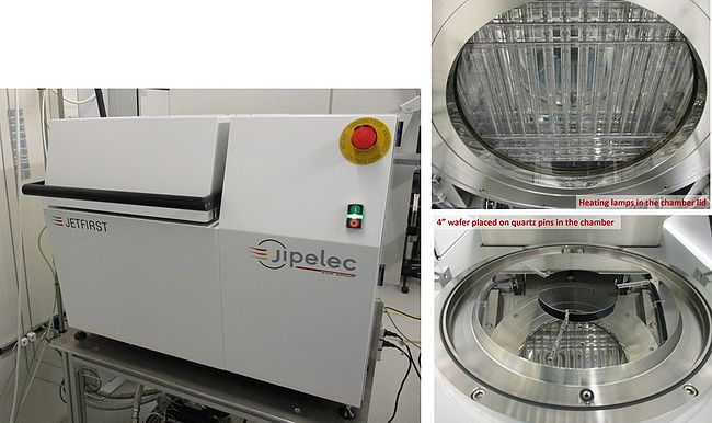
The chamber can be heated up very rapidly by the use of 18 infrared halogen lamps that are situated in the chamber lid. A quartz plate is placed below the lamps, i.e. between the lamps and the sample(s). Below the platen, there is an optical pyrometer aligned with the center of the substrate, that is placed on the bottom part of the chamber. The platen presents additional inlets where multiple thermocouples can be mounted. These details are exemplified in images below.

Jipelec JetFIRST 200 RTP (Rapid Thermal Processor/Annealer).
The main purpose of the machine is to anneal different samples very rapidly. Furthermore, the machine can be used for alloying of different materials.
The annealing is done in a process chamber on the machine, in which the samples are heated very rapidly by use of infra red lamps placed in the top of the chamber, directly above the sample(s). The chamber walls are cooled and remains cold during the annealing.
Samples can be wafers (2", 4", 6" and 8") or smaller samples made of different materials. In the process chamber, Si-based samples are normally placed on a 6" graphite susceptor and III-V and metals samples on a Si carrier wafer. Wafers can also be placed directly in the chamber.
The maximum annealing temperature is 1200 C. For temperatures above 700 C the annealing time is limited as can be seen in the table below.
The temperature is measured by either a thermocouple or an optical pyrometer . The temperature is regulated by a PID controller, thus the PID values will have to be optimized for each process and for each each susceptor or wafer size and thickness, annealing temperature, temperature ramping, pressure and gas flow settings etc. The responsible persons will help with the optimization of the PID parameters.
Annealings can be done at atmospheric pressure or in vacuum. It is also possible to apply a flow of either nitrogen or argon during the annealing, and forming gas (4 % H2/96 % N2) will be connected later.
The user manual, user APV, technical information and contact information can be found in LabManager:
| Purpose | Rapid thermal processor/annealer | |
|---|---|---|
| Process parameter range | Process temperature |
Annealing temperature:
Temperature ramp:
|
| Process pressure |
| |
| Gases on the system |
Process gases:
Purge gas:
| |
| Substrates | Batch size |
|
| Substrate materials allowed |
|
