Specific Process Knowledge/Thermal Process/RTP Jipelec 2
Feedback to this page: click here
THIS PAGE IS UNDER CONSTRUCTION
Jipelec - Rapid Thermal Processing

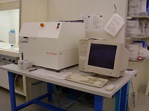
Jipelec JetFIRST 200 RTP (Rapid Thermal Processer/Annealer).
The main purpose of the machine is to anneal different samples very rapidly, or the machine can be used for alloying.
The machine consists of a process chamber, in which the annealing is done. Samples are placed on quartz pins, either on a graphite sucseptor or, Si dummy wafer or directly in the chamber in the process chamber.
Samples can be 6", 4" wafers or smaller samples made of different materials. In chamber, ht ehte
The maximum annealing temperature is 1200 C, and the heating is done by infrared lamps. Important: check the temperature limits in the table below.
Annnealings can be done at atmospheric pressure or in vacuum. It is also possible to apply a flow of either nitrogen or argon during the annealing.
In the chamber, sample are placed on quartz pins in the bottom of the chamber. 4" and 6" Si wafers can be placed directly on the quartz pins as show in the next picture, or these can be placed on a graphite susceptor. Smaller wafer and smaller samples can be placed on a Si dummy wafer or a graphite susceptor.
The
The Jipelec is a rapid thermal processing (RTP) oven. It is be used for fast and well-controlled annealing or alloying of samples. It is possible to use either a thermocouple or a pyrometer to control the temperature (of the sample carrier).
The user manual, technical information and contact information can be found in LabManager:
| Purpose | RTP annealing | |
|---|---|---|
| Process parameter range | Process Temperature |
|
| Process pressure |
| |
| Gases on the system |
| |
| Substrates | Batch size |
|
| Substrate materials allowed |
A carrier is always needed: For III-V materials a carbide carrier is used, and for other samples a silicon carrier wafer with 1 µm oxide is used
|
