Specific Process Knowledge/Thin film deposition/Lesker
Feedback to this page: click here

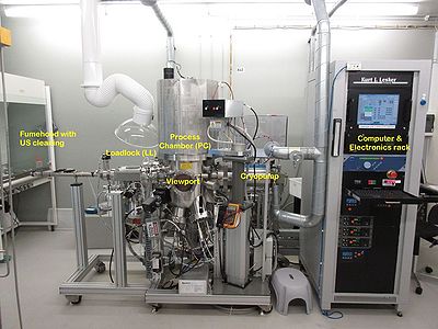
LESKER Sputter Tool
The purpose of the sputter is to deposit magnetic metals and dielectrica on a single 4" or 6" wafer at a time.
It can be a problem to take wafers from the sputter and into the other machines in the cleanroom, since it is not very clean. In principle the sputter should be the last step before you take your wafers out of the cleanroom. If you need to take process your wafers further please contact the PVD group so they can help you.
Lift-off of magnetic materials should never be done in the normal lift-off bath in RR4. It should always be done in the dedicated lift-off bath in the fumehood next to the sputter.
The user manual, user APV and contact information can be found in LabManager:
Sputter-System(Lesker) in LabManager
Materials for sputtering
- Gold (Au)
- Nickel (Ni)
- Silver (Ag)
- Silicon (Si)
- Iron (Fe)
- + many more (see list below or ask)
Contact the pvd-group if you have special needs (pvd@danchip.dtu.dk).
Sputter rate
The sputter rate depends on
- target material
- gun power (increasing power gives in general higher rate). Be aware of limitations on the power for different materials.
- chamber pressure (increasing pressure gives in general lower rate). Too low a pressure can make the plasma unstable.
- gas in chamber (Ar, N2, O2 or mixture).
In the tabel below (Relative Sputter rates) there a given a list of relative sputter rates for different materials (Al is set to 1). This means that You can estimate the sputter rate for a new material if you have the rate for another material under the same conditions. I think this only works for non-reactive sputtering (i.e. with Ar as the gas).
Thickness uniformity
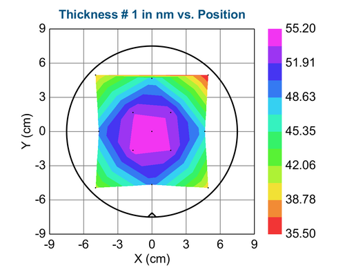
We have measured the thickness of a TiOx film deposited on a 6" si wafer.

Deposition parameters were:
| Recipe | source 3 with oxygen |
|---|---|
| time | 600 s |
| Gas | O2/Ar Ratio 10/100 |
| Pressure | 3 mtorr |
| Gun | 3 |
| Target | Ti |
| Power | 200 W |
| Voltage | 370V |
| Purpose | Deposition of magnetic metals and dielectrica |
|
|---|---|---|
| Performance | Film thickness |
|
| Deposition rates |
| |
| Process parameter range | Process Temperature |
|
| Process pressure |
| |
| Process Gases |
| |
| Substrates | Batch size |
|
| Substrate material allowed |
| |
| Material allowed on the substrate |
|
Film quality optimization
By Bjarke Thomas Dalslet @Nanotech.dtu.dk
The Lesker CMS 18 sputter system can produce films in a wide range of qualities. The quality of a film depends strongly on the substrate (lattice matching), but also on the energy the sputtered material can utilize for annealing.
Strain estimations was done on 30 nm NiFe thin films using low angle x-ray diffraction, for various substrates. It was found that the strain of the film influenced the resistance (R) and anisotropic magneto resistance (AMR) of the films (this relationship is also documented in literature); A Ta interface layer reduced R and increased AMR on both Si and SiO substrates while reducing strain.
This study was then done on 30 nm NiFe thin films deposited on 3 nm Ta on top of a SiO substrate, using R and AMR as an indication of strain. As seen in the tables, applying a substrate bias increases AMR and conductance (1/R). An equivalent effect is seen when heating the substrate during deposition. This heating can also be done after deposition without loosing the effect.
| Name | Substrate bias (W) | AMR | 1/R (S) | Crystal strain |
| 0029 NiFe3_stack_RF20 | 20 | 0.02724278 | 1.308044474 | |
| 0018_NiFe1_stack_RF | 10 | 0.025850358 | 0.898311175 | |
| 0030 NiFe3_stack | 0 | 0.020103598 | 0.71772052 | 0.8 |
| Name | Temperature (C) | AMR | 1/R (S) | Crystal strain |
| 0030 NiFe3_stack | 25 | 0.020103598 | 0.71772052 | 0.8 |
| BDT-NiFe1-blank30 | 200 | 0.019319002 | 1.095770327 | |
| BTD-NiFe-Blank22 | 250 | 0.021768497 | 1.047668937 | |
| BTD-NiFe-Blank14 | 300 | 0.02983617 | 1.724137931 | |
| BTD-NiFe-Blank13 | 350 | 0.033944331 | 1.887504719 | |
| BTD-NiFe-Blank15 | 400 | 0.031176801 | 1.655903295 | 0.2 |
| BTD-NiFe-Blank16 | 450 | 0.030843457 | ||
Surface roughness optimization
By Bjarke Thomas Dalslet @Nanotech.dtu.dk
The Lesker CMS 18 sputter system provides thin films of varying surface roughness. This roughness was verified to be dependent on the sputtered material, sputter mode (DC or RF) and the substrate bias strength. Other probable factors include sputter power and pressure. Below is a table for three cases.
The "From SiO target (RF sputter)" study was done on clean Si substrates. The sputter power was 157W and the pressure 3.5 mTorr using RF sputtering of a SiO target. The film thicknesses were around 42 nm.
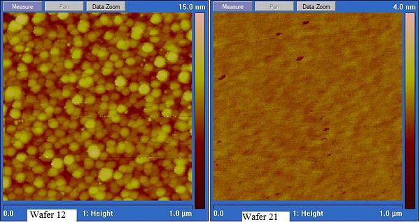
The "From Si target (DC sputter)" study was done on clean Si substrates. The sputter pressure 3 mTorr using DC reactive sputtering of a Si target. Oxygen was added to the argon sputter gas. Above 10% O the gun seems to oxidize (at this sputter power). Figure 1 shows the difference in AFM images between no RF bias (wafer 12) and RF bias (Wafer 21).
The "Ta" study was done on clean Si substrates. The sputter pressure was 3 mTorr using DC sputtering of a Ta target. Some O was added to wafer 25 and 26 to make TaO. In order to get fully oxidized films, up to 30-45% O should be added. Consult the thesis of Carsten Christensen for details on TaO.
Other studies on metals (NiFe/MnIr) show only limited effect of the substrate bias on the roughness.
From SiO2 target (RF sputter)
| Wafer nr | RF bias (W) | Reactive O2 (%) | Power(W) | Rq (RMS) (nm) | Thickness |
| 3 | 0 | 0 | 157 | 0.902 | |
| 6 | 5 | 0 | 157 | 0.499 | 44 |
| 7 | 10 | 0 | 157 | 0.142 | 42 |
| 8 | 15 | 0 | 157 | 0.422 | 40 |
From Si target (DC sputter)
| Wafer nr | RF bias (W) | Reactive O2 (%) | Power(W) | Rq (RMS) (nm) | Thickness |
| 12 | 0 | 5 | 135 | 1.44 | 123 nm (ellipsometry) |
| 13 | 0 | 9 | 130 | 1.32 | 98 nm (ellipsometry) |
| 14 | 0 | 13 | 100 | 1.37 | 71.5 nm (ellipsometry) |
| 15 | 10 | 9 | 90 | 0.984 | 56.25 nm (ellipsometry) |
| 21 | 20 | 9 | 90 | 0.112 | |
| 22 | 15 | 9 | 90 | 0.509 |
Ta
| Wafer nr | RF bias (W) | Reactive O2 (%) | Power(W) | Rq (RMS) (nm) | Thickness |
| blank1 | 0 | 0 | 180 | 0.209 | |
| 16 | 10 | 0 | 180 | 0.36 | 56 |
| 24 | 20 | 0 | 180 | 0.357 | |
| 25 | 20 | 9 | 180 | 0.202 | 110 |
| 26 | 20 | 5 | 180 | 0.194 | 95 |
| 27 | 15 | 0 | 180 | 0.413 | |
| 28 | 25 | 0 | 180 | 0.164 | |
| 31 | 30 | 0 | 180 | 0.3 |

Oxide insulation analysis
by Bjarke Thomas Dalslet @Nanotech.dtu.dk
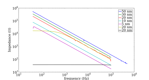
The wafers in this analysis consisted of a Si substrate with no native oxide. A layer of SiO was reactively sputtered (9% O2 90 W 3.5 mTorr). After that, using a shadow mask, 200nm thick gold rectangles was electro deposited on top of the oxide. Gold was also electro deposited on the back side. Then the impedance as a function of frequency was recorded.
The figure shows the measurements for different oxide thicknesses. Most of the measurements show perfect capacitors, although for illustration measurements with a few pinholes and with many pinholes is also shown for the 20 nm sample.
The success rate for the different thicknesses can be seen in the table, together with the number of samples measured and the number of perfect capacitors.
It is possible to make perfect capacitors with oxide thicknesses down to and including 5 nm and possibly even thinner, although the failure rate increases. Bear in mind, though that each structure measured here has an area of 8 mm2 - for a 1 mm2 structure the failure rate would be much lower, assuming the short circuits are not located on the sides of the structures.
| Name | Thickness [nm] | # samples measured | # good capacitors | Success rate [%] |
| 38 | 5 | 11 | 1 | 9 |
| 39 | 10 | 10 | 2 | 20 |
| 40 | 20 | 7 | 3 | 43 |
| 41 | 30 | 7 | 7 | 100 |
| 37 | 50 | 7 | 7 | 100 |
List of available targets for the Sputter-System(Lesker) (03 June 2013)
| Deposition material | target thickness | Purity |
| Ag | 0,250" | 99,9% |
| Al | 0,250" | 99,99% |
| Au | 0,125" | 99,999% |
| Co | 0,0625" | 99,95% |
| Cr | 0,125" | 99,95% |
| Cu | 0,250" | 99,99% |
| Fe | 0,0625" | 99,9% |
| Ge | 0,250" | 99,999% |
| Mg | 0.250" | 99,95% |
| Mo | 0,250" | 99,95% |
| Nb | 0,250" | 99,95% |
| Ni | 0,125" | 99,9% |
| Pd | 0,125" | 99,95% |
| Pt | 0,125" | 99,95% |
| Ru | 0,125" | 99,95% |
| Si, Undoped | 0,250" | 99,999% |
| Ta | 0,250" | 99,95% |
| Te | 0,250" | 99,999% |
| Ti | 0,250" | 99,7% |
| Al2O3 | 0,125" + Cu backing plate | 99,99% |
| Al2O3 | 0,250" | 99,99% |
| Al/Cu99,5/0,5% | 0,250" | 99,99% |
| Co/Fe 50/50% | 0,0625" | 99,95% |
| Co/Fe 80/20% | 0,0625" | 99,95% |
| Co/Fe 90/10% | 0,0625" | 99,95% |
| Cr2O3 | 0,125" + Cu backing plate | 99,8% |
| Cu/Ti/25% | 0,125" | 99,99% |
| Fe/Mn 50/50% | 0,250" | 99,95% |
| ITO (In2O3/SnO2) 90/10% | 0,125" | 99,99% |
| Mn/Ir80/20% | 0,125" | 99,9% |
| MgO | 0,125" | 99,95% |
| Ni/Co50/50% | 0,0625" | 99,95% |
| Ni/Co 50/50% | 0,125" | 99,95% |
| Ni/Fe 80/20% | 0.125" | 99,95% |
| NiV 93/7% | 0,250" | 99,95% |
| Si3N4/MgO 2% | 0,125" | 99,9% |
| SiO2 | 0,125" | 99,995% |
| SiO2 | 0,250" | 99,995% |
| Ta2O5 | 0,125" | 99,900% |
| AZO (ZnO/Al2O3) 98%/2% | 0,125" | 99,99% |
| ZnO | 0.250" | 99,999% |
| ZrO(2)/Y(2)O(3) | 99,900% |
Relative Sputter rates
To use these charts, locate the material for which known conditions are available. Then multiply the rate by the relative factors to arrive at the estimated rate for the new material. For example, with previous data showing 3.5Å/s Aluminum at 100W, then Titanium at similar conditions will generate approximately
- (0.53/1.00)·3.5 Å/s ≅ 2 Å/s
The rates in this table are calculated based on a 500V cathode potential. As the power is increased greater than two times the original rate, then the relative rate will drop slightly (up to 10%). For example, Aluminum at 250W
- Al250W = 0.9·Al100W·(P1/P0)
- 0.9·3.5 Å/s·(250/100) ≅ 7.4 Å/s
The rates in the ceramics table assume the use of an RF power supply and account for the partial duty cycle of the RF generator as compared to a DC supply.
Metals and semiconductors
| Deposition material | name | Relative depostion rate |
| Ag | Silver | 2.88 |
| Al | Aluminum** | 1.00 |
| Au | Gold | 1.74 |
| Be | Beryllium | 0.21 |
| C | Carbon | 0.23 |
| Cu | Copper | 1.42 |
| GaAs | Gallium Arsenide {100} | 1.03 |
| GaAs | Gallium Arsenide {110} | 1.03 |
| Ge | Germanium | 1.50 |
| Mo | Molybdenum | 0.66 |
| Nb | Niobium | 0.76 |
| Pd | Palladium | 1.77 |
| Pt | Platinum | 1.00 |
| Re | Rhenium | 0.84 |
| Rh | Rhodium | 1.16 |
| Ru | Ruthenium | 0.98 |
| Si | Silicon | 0.60 |
| Sm | Samarium | 1.74 |
| Ta | Tantalum | 0.67 |
| Th | Thorium | 1.31 |
| Ti | Titanium | 0.53 |
| V | Vanadium | 0.50 |
| W | Tungsten | 0.57 |
| Y | Yttrium | 1.53 |
| Zr | Zirconium | 0.88 |
Oxides and Ceramics
| Deposition material | name | Relative depostion rate |
| Al2O3 | Alumina | 0.05 |
| SiC | Silicon Carbide | 0.22 |
| SiO2 | Silicon Dioxide | 0.21 |
| TaC | Tantalum Carbide | 0.09 |
| Ta2O5 | Tantalum Pentoxide | 0.39 |
Magnetic Materials
| Deposition material | name | magn. | Relative depostion rate |
| Co | Cobalt | Low | 0.73 |
| Cr | Chromium | Med | 0.87 |
| Fe | Iron | High | 0.57 |
| Mn | Manganese | Med | 0.14 |
| Ni | Nickel | Low | 0.86 |
| Ni80Fe20 | Permalloy | High | 0.80 |


