Specific Process Knowledge/Characterization/Tencor P17: Difference between revisions
| Line 16: | Line 16: | ||
== Process information == | == Process information == | ||
*Info about [[Specific Process Knowledge/Characterization/Dektak XTA#Measurement Accuracy |measurement accuracy]] (''measured with Dektak XTA'') | *Info about [[Specific Process Knowledge/Characterization/Dektak XTA#Measurement Accuracy |measurement accuracy]] (''measured with Dektak XTA'') | ||
*Vendor's description of | *Vendor's description of [https://labmanager.dtu.dk/view_binary.php?fileId=6385 instrument specs including reproducibility and flatness of scans] (''requires login as it seems not freely available from vendor's website'') | ||
*Using the analysis software: [[Specific Process Knowledge/Characterization/Tencor P17#Apex Software for Data Analysis|Apex software access & tips]] | *Using the analysis software: [[Specific Process Knowledge/Characterization/Tencor P17#Apex Software for Data Analysis|Apex software access & tips]] | ||
*Tips on making [https://labmanager.dtu.dk/view_binary.php?fileId=5543 2D stress measurements] ''(requires login)'' | *Tips on making [https://labmanager.dtu.dk/view_binary.php?fileId=5543 2D stress measurements] ''(requires login)'' | ||
Most users will want to make 3D stress measurements, which is described in the regular Nanolab manual for the P17, also found on LabManager. It counts as "3D" if you wish to make 2 perpendicular scans. A "2D" stress scan means a single line scan per wafer - the software does not allow rotation of the stage for this type of scan. | Most users will want to make 3D stress measurements, which is described in the regular Nanolab manual for the P17, also found on LabManager. It counts as "3D" if you wish to make 2 perpendicular scans. A "2D" stress scan means a single line scan per wafer - the software does not allow rotation of the stage for this type of scan. | ||
*Vendor's document on 2D stress measurements (also somewhat informative for 3D stress measurements) including info on | *Vendor's document on 2D stress measurements (also somewhat informative for 3D stress measurements) including info on the automatic fitting to calculate the local radius of the wafer: [https://www.kla.com/wp-content/uploads/KLA_AppNote_Stylus_2D_Stress.pdf]. | ||
<br> | <br> | ||
Revision as of 12:26, 7 July 2025
The content on this page, including all images and pictures, was created by DTU Nanolab staff, unless otherwise stated.
Feedback to this page: click here
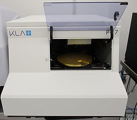
Tencor P17 (Stylus Profiler)
The P17 Stylus Profiler from KLA Tencor is used in a similar manner to the Dektak XTA profiling surfaces with structures in the micro- and submicrometer range as well as for measuring stress. Both of these tools are inside the cleanroom.
Compared to the DektakXT, the P17 has more advanced options for stress measurements: It allows the user to measure a stress map with up to 5° radial resolution. Programming and analyzing a sequence of predefined scans in fixed locations on a wafer is also easier and the manual for doing it much better for the P17 than for the DektakXT. A disadvantage of the P17 is that is can be hard to locate structures as the maximum field of view of the camera is 1x1.5 mm. We recommend having a map of the sample design available so you can easily locate the features of interest. Otherwise the P17 is easy to use, fast, and accurate, just like the DektakXT.
The user manual, quality control procedure and results, technical information and contact information can be found in LabManager.
Process information
- Info about measurement accuracy (measured with Dektak XTA)
- Vendor's description of instrument specs including reproducibility and flatness of scans (requires login as it seems not freely available from vendor's website)
- Using the analysis software: Apex software access & tips
- Tips on making 2D stress measurements (requires login)
Most users will want to make 3D stress measurements, which is described in the regular Nanolab manual for the P17, also found on LabManager. It counts as "3D" if you wish to make 2 perpendicular scans. A "2D" stress scan means a single line scan per wafer - the software does not allow rotation of the stage for this type of scan.
- Vendor's document on 2D stress measurements (also somewhat informative for 3D stress measurements) including info on the automatic fitting to calculate the local radius of the wafer: [1].
Acceptance test
- The acceptance test carried out for the P17: File:Acceptance test p17 final_no-names.pdf
- Vendor's own conformity test results after installation (requires login).
Performance and Process Parameters

| Purpose | Profiler for measuring microstructures |
|
|---|---|---|
| Performance | Scan range X Y |
Line scan X: 20 µm to 200 mm in a single scan. No stitching. Map scan XY: In principle any rectangle that can be inscribed in a 200 mm circle, but resolution is limited to max. 4 million points and scanning is slow. In practice to get good resolution scan a very small area (e.g., 100 x 500 µm) |
| Scan range Z |
50 nm to 900 µm. It is possible to measure smaller steps but not recommended as the results may not be accurate. | |
| Resolution X Y |
Down to 0.025 µm in theory, but the tip radius is 2 µm, so the meaningful resolution is at the same order of magnitude | |
| Resolution Z |
0.01 Å, 0.08 Å, or 0.6 Å according to the manufacturer for ranges 13 µm, 131 µm, and 1 mm. Note the smallest of these values are purely theoretical as they are far below the lab's noise level. | |
| Height accuracy z (95 % confidence) |
~ 2 % for the smallest range for a 1 micron step and ~ 1 % for a 25 micron step for well-defined steps that are easy to measure (read about reducing and estimating the measurement uncertainty here) | |
| Max scan depth as a function of trench width W |
0.87*(W[µm]-2µm) = tan(60o)/2*(W[µm]-2µm) (empirically validated by Nanolab staff) | |
| Hardware settings | Tip radius |
|
| Substrates | Substrate size |
|
| Substrate materials allowed |
|
Apex Software for Data Analysis
The Tencor-KLA P17 stylus profiler comes with advanced data analysis software called APEX. We have an extra license for the software on a computer in the basement of building 346. The computer is located at the back of room 904 between the XRD Powder and the AFM. At the moment remote access is not possible, but you are able to access your files on the M-drive from the computer. Let us know if you would like us to find a solution for remote access and/or would like us to move the analysis computer to a room with daylight, as we are not sure how many of you would actually like to use the software.
To use Apex, your data must be in a format that Apex can open. For line profiles that means you have to open the data in the Profiler Software first, which can only be done on the P17 computer in the cleanroom. With the data open or selected, press the Apex button and save it in Apex in a native format. It is also possible to check a box in the scan recipe that makes it possible to open the data in Apex automatically (see the Profiler Help document for more details or ask staff). Finally some data formats (e.g., 3D maps and 3D stress data) can always be opened in Apex.
How to use the software

There are a number of tutorials and a help document which you will find when you open the program. There is also a small introduction as an appendix to the P17 help document (requires login).
Apex offers many formats for saving the data in nice reports and various options for exporting data.
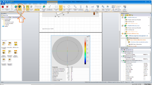
If Apex has automatically generated a surface from your line profiles of data, it is possible to view the underlying profiles by right-clicking on the surface and choosing Points Drawing instead of Lines Drawing or finding the same option (Points drawing) in the top ribbon. See figure on the right.
Please contact characterization@nanolab.dtu.dk if you have any questions or helpful tips.
