Specific Process Knowledge/Lithography: Difference between revisions
mNo edit summary |
m TPT udated, most links checked and updated |
||
| Line 3: | Line 3: | ||
'''Feedback to this page''': '''[mailto:labadviser@nanolab.dtu.dk?Subject=Feed%20back%20from%20page%20http://labadviser.nanolab.dtu.dk/index.php?title=Specific_Process_Knowledge/Lithography click here]''' | '''Feedback to this page''': '''[mailto:labadviser@nanolab.dtu.dk?Subject=Feed%20back%20from%20page%20http://labadviser.nanolab.dtu.dk/index.php?title=Specific_Process_Knowledge/Lithography click here]''' | ||
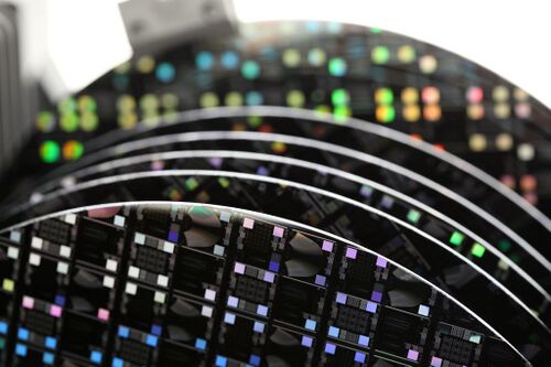
[[Image:DUV_wafers.jpg|500px|frameless|right|]] | [[Image:DUV_wafers.jpg|500px|frameless|right|]] | ||
| Line 273: | Line 271: | ||
*[http://onlinelibrary.wiley.com/doi/10.1002/9781119990413.ch9/pdf Franssila, 2010, Chapter 9: Optical Lithography] | *[http://onlinelibrary.wiley.com/doi/10.1002/9781119990413.ch9/pdf Franssila, 2010, Chapter 9: Optical Lithography] | ||
*[http://onlinelibrary.wiley.com/doi/10.1002/9781119990413.ch10/pdf Franssila, 2010, Chapter 10: Advanced Lithography] | *[http://onlinelibrary.wiley.com/doi/10.1002/9781119990413.ch10/pdf Franssila, 2010, Chapter 10: Advanced Lithography] | ||
*[http://www.cnf.cornell.edu/cnf_spietoc.html Handbook of Microlithography, Micromachining, and Microfabrication, Chapter 2: E-beam Lithography] | *[http://www.cnf.cornell.edu/cnf_spietoc.html Handbook of Microlithography, Micromachining, and Microfabrication, Chapter 2: E-beam Lithography] | ||
*[http://onlinelibrary.wiley.com/doi/10.1002/9781118557662.ch3/summary Stefan Landis,Lithography, Chapter 3: E-beam Lithography] | *[http://onlinelibrary.wiley.com/doi/10.1002/9781118557662.ch3/summary Stefan Landis,Lithography, Chapter 3: E-beam Lithography] | ||
*[https://www.microchemicals.com/downloads/application_notes.html Application notes] from MicroChemicals GmbH, e.g. [https://www.microchemicals.com/ | *[https://www.microchemicals.com/downloads/application_notes.html Application notes] from MicroChemicals GmbH, e.g. [https://www.microchemicals.com/dokumente/application_notes/lithography_trouble_shooting.pdf Lithography Trouble-Shooter] | ||
| Line 310: | Line 306: | ||
*[https://www.youtube.com/watch?v=btinNzYnLnY Training Video: Manual Puddle Developer] | *[https://www.youtube.com/watch?v=btinNzYnLnY Training Video: Manual Puddle Developer] | ||
'''Playlists on YouTube:''' | '''Playlists on YouTube:''' | ||
*[https://www.youtube.com/ | *[https://www.youtube.com/playlist?list=PLjWVU97LayHAiCabstMfAUeeWyQoQI_cV Maskless aligner (MLA) training videos] | ||
*[https://www.youtube.com/ | *[https://www.youtube.com/playlist?list=PLjWVU97LayHCX4sz2AH_YiPbNRmkrBYe5 Lithography equipment training videos (old)] | ||
| Line 317: | Line 313: | ||
'''<big>Manuals</big>'''<br> | '''<big>Manuals</big>'''<br> | ||
'''NB: Access to manuals require login''' | '''NB: Access to manuals require login''' | ||
*Automatic Spin Coater: [ | *Automatic Spin Coater: [https://labmanager.dtu.dk/d4mb/show.php?dokId=4140&mach=359 Spin Coater: Gamma UV] | ||
*Manual Spin Coater: [ | *Manual Spin Coater: [https://labmanager.dtu.dk/d4mb/show.php?dokId=5073&mach=362 Spin Coater: Labspin 02] or [https://labmanager.dtu.dk/d4mb/show.php?dokId=5074&mach=387 Spin Coater: Labspin 03] | ||
*UV Mask Aligner: [http://labmanager.dtu.dk/d4Show.php?id=3822&mach=339 Aligner: MA6 - 2 | *UV Mask Aligner: [http://labmanager.dtu.dk/d4Show.php?id=3822&mach=339 Aligner: MA6 - 2] | ||
*Automatic Puddle Developer: [ | *Automatic Puddle Developer: [https://labmanager.dtu.dk/d4mb/show.php?dokId=3561&mach=329 Developer: TMAH UV-lithography] | ||
*Manual Puddle Developer: [ | *Manual Puddle Developer: [https://labmanager.dtu.dk/d4mb/show.php?dokId=3274&mach=324 Developer: TMAH Manual] | ||
*Manual E-beam Developer: [ | *Manual E-beam Developer: [https://labmanager.dtu.dk/d4mb/show.php?dokId=20599&mach=527 Developer: E-beam Manual] | ||
Revision as of 09:43, 7 February 2025
The content on this page, including all images and pictures, was created by DTU Nanolab staff, unless otherwise stated.
Feedback to this page: click here

There are four different types of lithography available at DTU Nanolab:
Comparing lithography methods at DTU Nanolab
| UV Lithography | DUV Stepper Lithography | E-beam Lithography | Nano Imprint Lithography | |
|---|---|---|---|---|
| Generel description | Pattern transfer via ultraviolet (UV) light | Pattern transfer via deep ultraviolet (DUV) light | Patterning by electron beam | Pattern transfer via hot embossing (HE) |
| Pattern size range |
~0.6 µm and up |
~200 nm and up |
~12 nm - 1 µm |
~20 nm and up |
| Resist type |
UV sensitive:
|
DUV sensitive
|
E-beam sensitive
|
Imprint polymers:
|
| Resist thickness range |
~0.5 µm to 200 µm |
~50 nm to 2 µm |
~30 nm to 1 µm |
~ 100 nm to 2 µm |
| Typical exposure time |
10 s - 3 min pr. wafer using mask aligners |
Process dependent:
Throughput is up to 60 wafers/hour |
Process dependent:
time [s] = Q*a/I |
Process dependent, including heating/cooling rates |
| Substrate size |
|
|
We have cassettes fitting:
Only one cassette can be loaded at a time |
|
| Allowed materials |
Any standard cleanroom material |
Any standard cleanroom material |
Any standard cleanroom material, except:
|
Any standard cleanroom material |
Equipment Pages
|
|
||
Lithography Tool Package Training
DTU Nanolab offers a Tool Package Training in Lithography (TPT Lithography). You are required to pass this course, in order to get access to the lithography equipment inside the DTU Nanolabs cleanroom facility. The course includes theory on lithographic processes and training videos for specific equipment. The theory part consists of lecture videos followed by quizzes for each section. Once that part has been completed successfully, you can begin the online training for the lithography equipment you need to use. After completing the online training, you can request hands-on training for the lithography equipment inside the cleanroom via training@nanolab.dtu.dk.
The course is available via DTU Learn. You sign up for the course by enrolling yourself in the course here.
Course Description
- Online lecture videos
- Quizzes for each section
- Equipment-related training videos
- Hands-on training
Hands on training can be requested via training@nanolab.dtu.dk.
Learning objectives
Learn about the fundamentals of lithography processing in a cleanroom fabrication lab:
- Coating
- Exposure
- Development
- Resist, substrates and pre-treatment
- Post-lithography steps
Knowledge and Information about Lithography
