Specific Process Knowledge/Thermal Process/RTP Jipelec 2: Difference between revisions
| Line 117: | Line 117: | ||
|style="background:LightGrey; color:black"| | |style="background:LightGrey; color:black"| | ||
*Chips on carrier | *Chips on carrier | ||
*100 mm or 150 mm wafers | *50 mm, 100 mm or 150 mm wafers | ||
|style="background:WhiteSmoke; color:black;" align="left"| '''Small samples''' must be '''placed''' on '''dedicated carrier wafers'''. These '''do not need to and should not be''' bonded to the carriers. | |style="background:WhiteSmoke; color:black;" align="left"| '''Small samples''' must be '''placed''' on '''dedicated carrier wafers/susceptors'''. These '''do not need to and should not be''' bonded to the carriers. | ||
|- | |- | ||
| style="background:Silver; color:black"|Allowed materials | | style="background:Silver; color:black"|Allowed materials | ||
|style="background:LightGrey; color:black"| | |style="background:LightGrey; color:black"| | ||
*Silicon | *Silicon | ||
*Silicon | *Silicon oxides and nitrides | ||
* | *Quartz | ||
*Metals - ask for permisson | |||
*III-V materials - '''these cannot be heated above 450 °C,''' otherwise it can lead to outgassing of toxic gases. For that reason, '''III-V samples are limited to a maximum process temperature of 440 °C.''' | |||
|style="background:WhiteSmoke; color:black;" align="left"| During previous testing, '''silicon nitride''' and '''aluminum oxide''' were only used as '''coating/masking materials''' and have been proven capable of sustaining this type of high temperature processing. | |style="background:WhiteSmoke; color:black;" align="left"| During previous testing, '''silicon nitride''' and '''aluminum oxide''' were only used as '''coating/masking materials''' and have been proven capable of sustaining this type of high temperature processing. | ||
|- | |- | ||
Revision as of 16:01, 6 November 2023
Feedback to this page: click here
This page is written by DTU Nanolab internal
THIS PAGE IS UNDER CONSTRUCTION
RTP2 Jipelec - Rapid Thermal Processor

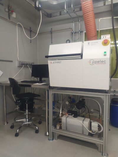
The main purpose of the RTP2 Jipelec (Jipelec JetFirst 200 RTP) is to perform thermal processes, using faster heating rates and shorter process durations when compared to conventional methods. This is called rapid thermal processing (RTP) and can be used to treat different types of samples.
Rapid thermal processing typically includes RTA, i.e. Rapid Thermal Annealing, where samples are heated up very rapidly in a nitrogen or argon atmosphere. Contact alloying and RTN, i.e. Rapid Thermal Nitridation, might also be possible for some samples.
The Set-Up
The machine consists of a reactor chamber, in which different samples can be processed/annealed at temperatures up to 1200 °C.
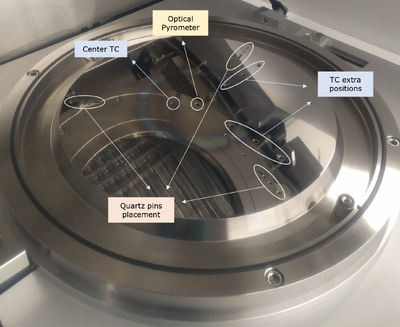
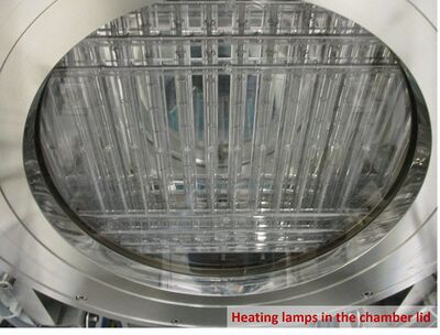
The chamber can be heated up very rapidly by the use of 18 infrared halogen lamps that are situated in the chamber lid. A quartz plate is placed below the lamps, i.e. between the lamps and the sample(s). Below the platen, there is an optical pyrometer aligned with the center of the substrate, that is placed on the bottom part of the chamber. The platen presents additional inlets where multiple thermocouples can be mounted. These details are exemplified in the images on the right.
[[|400px|thumb|Schematic representation of the RTP2 Jipelec reactor. Image: DTU Nanolab]]

The lamps are divided in three zones so that a uniform temperature can be obtained over the substrate. During the heating, the quartz window below the lamps will get warm. However, the chamber walls are cooled by a cooling water flow and thus remain cold to prevent sample contamination. As already mentioned, the cooling unit is located under the machine. The lamps are cooled by cooling fans (no noisy compressed air cooling like in the old Jipelec RTP). The halogen lamps and the quartz plate are visible in the image below.

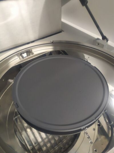
The samples are placed above the round metal plate in the bottom of the chamber, i.e. below the halogen lamps. The substrates are meant to be placed on top of three quartz pins. Depending on the type and size of the substrate, there are three types of quartz pins available (for the SiC-coated graphite susceptor, a 100 mm wafer and for a 150 mm wafer). Nonetheless, the susceptor should always be used, when possible (except for 8" wafers).

Temperature Measurement and Control
Samples and Process Specifications
| Specifics | Range | Comments | |
|---|---|---|---|
| Temperature | Pyro Control |
|
|
| Thermocouple Control |
|
||
| Process gas | Argon (Ar) |
|
|
| Nitrogen (N2) |
|
Limited use. | |
| Forming gas (4% H2/ 96% N2) |
|
Gas line not connected yet. | |
| Nitrogen purge (N2) |
|
Do not use for processing. | |
| Pressure | No vacuum |
|
|
| Vacuum |
|
5/6 mbar, if minimum gas flow during process. | |
| Process time
(Check image below) |
At 1200 oC |
|
|
| At 1100 oC |
|
||
| At 1000 oC |
|
||
| Heating rate |
|
Different heating rates can be set under temperature control, as well as the step duration. | |
| Substrates | Batch size |
|
|
| Substrate size |
|
Small samples must be placed on dedicated carrier wafers/susceptors. These do not need to and should not be bonded to the carriers. | |
| Allowed materials |
|
During previous testing, silicon nitride and aluminum oxide were only used as coating/masking materials and have been proven capable of sustaining this type of high temperature processing. | |
Additional information
The user manual, user APV, technical and contact information can be found in LabManager: RTP2 Jipelec
