LabAdviser/314/Microscopy 314-307/Technique/Holo: Difference between revisions
Created page with "'''Feedback to this page''': '''[mailto:labadviser@nanolab.dtu.dk?Subject=Feed%20back%20from%20page%20http://labadviser.nanolab.dtu.dk/index.php/LabAdviser/314/Technique/X-ray..." |
mNo edit summary |
||
| Line 7: | Line 7: | ||
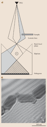
Off-axis electron holography is a transmission electron microscopy technique that is sensitive to the phase of the electrons passing through the specimen. The measurement of phase changes of electrons is very important for measuring material properties like mean inner potential and built-in potential. It is also very important in measuring charge distribution across specimens at a high spatial resolution. In this technique a part of the electron beam passes through the specimen and the other part passes through vacuum. A biprism wire (see the below figure) in the plane of the SAD apertures is held at a fixed potential and this creates an interference pattern between the electrons passing through the specimen and vacuum. | Off-axis electron holography is a transmission electron microscopy technique that is sensitive to the phase of the electrons passing through the specimen. The measurement of phase changes of electrons is very important for measuring material properties like mean inner potential and built-in potential. It is also very important in measuring charge distribution across specimens at a high spatial resolution. In this technique a part of the electron beam passes through the specimen and the other part passes through vacuum. A biprism wire (see the below figure) in the plane of the SAD apertures is held at a fixed potential and this creates an interference pattern between the electrons passing through the specimen and vacuum. | ||
[[file:Off-axis_Holo_sketch.png|thumb|150px|center|Schematic of the set-up for off-axis electron holography and example image]] | [[file:Off-axis_Holo_sketch.png|thumb|150px|center|Schematic of the set-up for off-axis electron holography and example image [https://link.springer.com/chapter/10.1007%2F978-3-030-00069-1_16]]] | ||
<br clear=all> | <br clear=all> | ||
The detailed procedure for obtaining electron holograms as well as thickness measurements using convergent beam electron diffraction is described below. The procedure has been used for obtaining holograms of GaAs nanowires, but it can be applied to other specimens. Some tips are also given at the end of this document. | The detailed procedure for obtaining electron holograms as well as thickness measurements using convergent beam electron diffraction is described below. The procedure has been used for obtaining holograms of GaAs nanowires, but it can be applied to other specimens. Some tips are also given at the end of this document. | ||
Revision as of 14:28, 21 April 2020
Feedback to this page: click here
Off-axis Electron Holography
Off-axis electron holography is a transmission electron microscopy technique that is sensitive to the phase of the electrons passing through the specimen. The measurement of phase changes of electrons is very important for measuring material properties like mean inner potential and built-in potential. It is also very important in measuring charge distribution across specimens at a high spatial resolution. In this technique a part of the electron beam passes through the specimen and the other part passes through vacuum. A biprism wire (see the below figure) in the plane of the SAD apertures is held at a fixed potential and this creates an interference pattern between the electrons passing through the specimen and vacuum.

The detailed procedure for obtaining electron holograms as well as thickness measurements using convergent beam electron diffraction is described below. The procedure has been used for obtaining holograms of GaAs nanowires, but it can be applied to other specimens. Some tips are also given at the end of this document.
