Specific Process Knowledge/Thin film deposition/Cluster-based multi-chamber high vacuum sputtering deposition system: Difference between revisions
| Line 234: | Line 234: | ||
==Load-lock== | ==Load-lock== | ||
The load-lock chamber is the only part of the tool which can be accesed by user. Ventilation and pumping takes approximately 5 min. The chamber has its own turbo pump. Inside there is a shelf - a cassete with 10 slots. The images below shows the load-lock set-up and sample mounting. The shelf is designed to handle 6-inch wafers, which has to be placed into dedicated carrier rings. Those rings with wafers can be introduced to the cassete - shelf. Different adapter-holders can be used for operating with 4-inch wafers and small chips. | The load-lock chamber is the only part of the tool which can be accesed by user. Ventilation and pumping takes approximately 5 min. The chamber has its own turbo pump. Inside there is a shelf - a cassete with 10 slots. The images below shows the load-lock set-up and sample mounting. The shelf is designed to handle 6-inch wafers, which has to be placed into dedicated carrier rings. Those rings with wafers can be introduced to the cassete - shelf. Different adapter-holders can be used for operating with 4-inch wafers and small chips. After the load-lock is puped it takes 6 min tol transfer the sample into the process chamber and 8 min to return back. | ||
<gallery caption="Deposition rates of HfO2 at different temperaturs. ALD window." widths="800px" heights="600px" | <gallery caption="Deposition rates of HfO2 at different temperaturs. ALD window." widths="800px" heights="600px" | ||
Revision as of 18:13, 22 March 2020
Feedback to this page: click here

Cluster-based multi-chamber high vacuum sputtering deposition system is a robotic cluster tool with two deposition chambers sharing the same distribution trasfer station and the load-lock. The equipment has been installed and accepted in clean-room during January 2020. The purpose of the tool is to deposite variety of materials using DC/RF/PulseDC/HIPIMS magnetron sputtering with or without RF substrate bias. In modul A or PC 1 (process chamber 1) it is possible to deposit any materials using 6 x 3” magnetrons sourses with N2 or O2 reactive gases. Modul B or PC 3 (process chamber 3) is dedicated to oxygen free materials - nitrides and metals. It is eqipted with 1 x 4” + 2 x 3” magnetrons and supplied with N2 process gas for reactive deposition. Both chambers allow heating of substrates up to 600 oC. The equipment is located in clean-room A-5 where the user can acces the cassete loader.
Manufacture: Kurt J. Lesker Company
Model: 2017 PRO Line PVD75 thin film deposition cluster system
The user manual, user APV and contact information can be found in LabManager:
Sputter-System Metal-Oxide(PC1)
Sputter-System Metal-Nitride(PC3)
Thin Film group thinfilm@nanolab.dtu.dk is responsible of the equipment
Target/Metal requests should be sent to metal@nanolab.dtu.dk
If you need a training on the machine please send your request to: training@nanolab.dtu.dk.
Sputtering deposition system set-up
The cluster sputter system is used for deposition of metals, magnetic metals and dielectrics on a single wafer 4" or 6" wafer or several small samples. Samples will be placed on the ten shelves cassette and loaded in the load lock module. After the load lock chamber is pumped down, the sample can be transferred to the desired process chamber. The sample will be rotated over the target and can be heated up to 600C while depositing the film. The system is equipped with two process chambers connected to a wafer transfer robot, and a load lock chamber.
- System set-up and power supply configuration.
-
 The system set-up showing the different operation chambers and power supplies network.
*HSM - High Strengh Magnet.
**RGA - Residual Gas Analyser.

Power suppliy configuration
Power supplies specifications presented in a table below.
| Power Supply ID | Type | Maximum output power (W) | Maximum output voltage (V) | Maximum output current (A) | Comments
|
|---|---|---|---|---|---|
| PC1 Power Supply 1 | RF | 300 | |||
| PC1 Power Supply 3 | DC | 500 | 1000 | 4 | |
| PC1 Power Supply 4 | DC | 500 | 1000 | 4 | |
| PC1 Power Supply 5 | Pulse DC | 2000 | 800 | 5 |
Max frequency: 100kHz |
| PC1 Power Supply 7 | RF (Substrate) | 100 | |||
| PC3 Power Supply 1 | RF | 300 | |||
| PC3 Power Supply 2 | Pulse DC | 2000 | 800 | 5 |
Max frequency: 100kHz |
| PC3 Power Supply 3 | DC to HiPIMS | 1500 | 1000 | 4 |
HiPIMS Unit
|
| PC3 Power Supply 5 | DC | 500 | 1000 | 4 |
|
| PC3 Power Supply 6 | RF (substrate) | 100 |
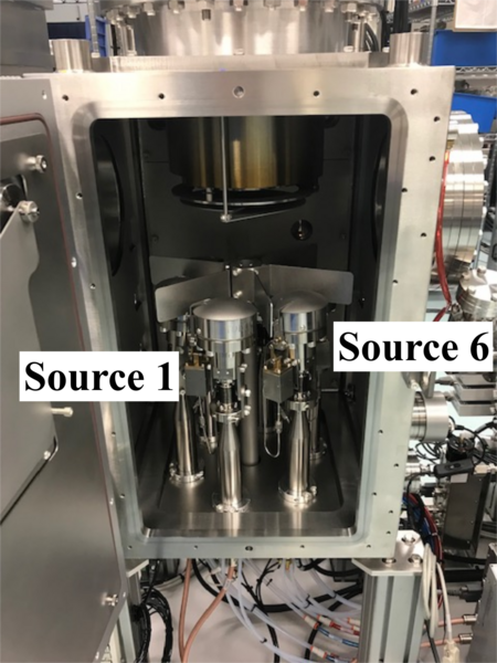
Sputter-System Metal-Oxide (PC1)
Chamber PC1 consists of six KJLC Torus® 3" magnetron sputtering sources with possibility of RF, DC, Pulse DC and HIPIMS sputtering. There are Argon, Nitrogen and Oxygen gas lines connected to this chamber. The chamber has a possibility to do the RF bias on a substrate, which can be used as substrate cleaning before the deposition or used during the deposition to alter the film properties. A deposition of magnetic material, which requires high strength magnet (HSM), has to be installed on source 3 in PC1. It is possible to do the co-sputtering (sputtering of two or more sources at the same time) as long as the sources are not sharing the same power supply.
- Process chamber (PC 1)
-
 Photography of the chamber.
 -
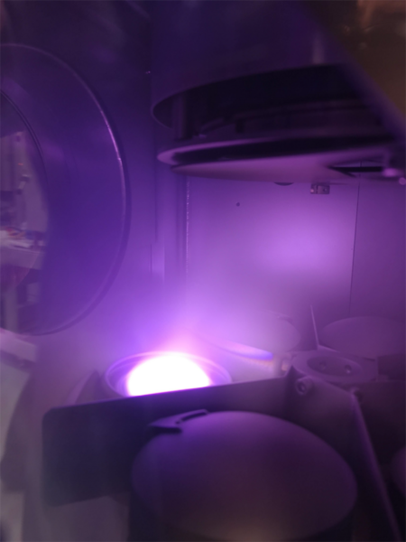 Deposition from source 2.


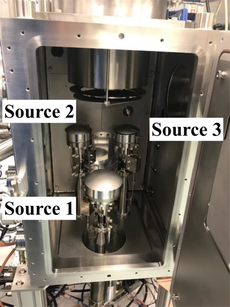
Sputter-System Metal-Nitride (PC3)
The second process chamber called PC3 consists of two KJLC Torus® 3" magnetron sputtering sources and one height-adjustable KJLC Torus® 4" magnetron sputtering source, also with the possibility of RF, DC, Pulse DC and HiPIMS sputtering. The chamber has a possibility to do the RF bias on a substrate, which can be used as substrate cleaning before the deposition or used during the deposition to alter the film properties. It is possible to do the co-sputtering (sputtering of two or more sources at the same time) as long as the sources are not sharing the same power supply. The chamber is equipped with a residual gas analyzer (RGA) that allows monitoring post-process chemical gas traces. In order to operate the analyzer, the chamber should be pumped to base pressure.
- Process chamber PC 3
-
 Photography of the chamber.
 -
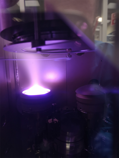 Deposition from source 2.


Distribution Chamber (Genmark robot)
The load-lock and process chambers PC1 and PC3 are all connected through the common distribution chamber. The robot arm can transfer the sample to the selected destination. During normal operation, the chamber is pumped to a base pressure ensuring the safe transfer of the sample between chambers and load-lock without breaking a vacuum.
- Distribution chamber (Robot). View from the service area.
-
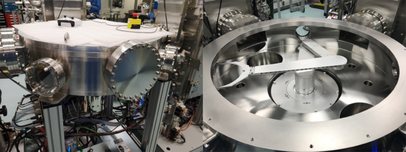 The photography of the distribution chamber with and without the top cover.

Load-lock
The load-lock chamber is the only part of the tool which can be accesed by user. Ventilation and pumping takes approximately 5 min. The chamber has its own turbo pump. Inside there is a shelf - a cassete with 10 slots. The images below shows the load-lock set-up and sample mounting. The shelf is designed to handle 6-inch wafers, which has to be placed into dedicated carrier rings. Those rings with wafers can be introduced to the cassete - shelf. Different adapter-holders can be used for operating with 4-inch wafers and small chips. After the load-lock is puped it takes 6 min tol transfer the sample into the process chamber and 8 min to return back.
- Deposition rates of HfO2 at different temperaturs. ALD window.
-
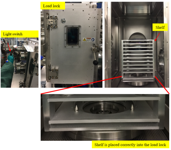 The load-lock chamber.
 -
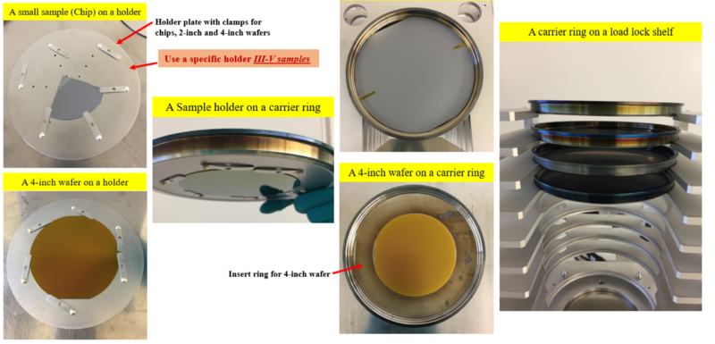 Sample holder, carrier ring and load lock shelf.


Attention! The shelf turns opposite side from when the carrier ring is loading in. Furthermore, the shelf has to be placed properly inside the load lock chamber. A carrier ring without sample should never be loaded in the load lock. The light in the load lock chamber can be turned on. The light switch is located on the left side of the load-lock. Process chambers PC 1 and PC 3 are also equipted with light switches.
Process information
Too high sputter power can cause target or sputter gun damage. Given the target/interface thermal limitations, such damage can be reduced/eliminated by using an appropriate maximum power. However, "appropriate" often equates to "low" and low power means low deposition rate. Once the appropriate power has been established for a given target/gun, never switch on and immediate increase power to that value! Always increase power slowly to its maximum value through a series of ramps. When the deposition run is complete, it is equally important to ramp down power at the same rate at ramp up, allowing the target to cool slowly to avoid thermal shock and the potential for target fracture.
Table below shows the maximum power and maximum ramp up/down power for all available materials:
| Target size | Target material | Maximum Power density (W/inch2) | Maximum Power (W) | Maximum Ramp up/down Power (W/s) | Comments
|
|---|---|---|---|---|---|
| 3 inch | Al | 150 | 1000 | 10 | DC/HiPIMS |
| Au | 100 | 700 | 10 | DC/HiPIMS | |
| Ag | 100 | 700 | 10 | DC/HiPIMS | |
| Cu | 200 | 1400 | 10 | DC/HiPIMS | |
| Ni | 50 | 350 | 10 | High strengh magnets/DC | |
| Ti | 50 | 350 | 10 | DC/HiPIMS | |
| Ge (Bonded) | 20 | 140 | 0.3 | DC/RF | |
| Si (Unbonded/Bonded) | 20 | 140 | 0.3 | RF
| |
| SiO2 (Bonded) | 20 | 140 | 0.3 | RF
| |
| ITO (Bonded) | 20 | 140 | 0.3 | RF/PDC
| |
| BaTiO3 (Bonded) | 20 | 140 | 0.3 | RF
| |
| NbTi | 50 | 350 | 10 | DC | |
| 4 inch | Al | 150 | 1800 | 10 | DC/HiPIMS |
Standard recipe performance
There are in total 76 developed and tested process recipes for general users (48 for PC1 and 28 for PC3). Starting the recipe the user can change te relevant process parameters: power, pressure, reactive gas ratio, rotation speed, substrate bias etc. In addition to the process recipes, there are also recipes for substrate heating and RF cleaning.
Bla bla
- Deposition rates of HfO2 at different temperaturs. ALD window.
-
 Deposition rate of HfO2 at 150 oC. Substrate: Silicon 6" wafer with native oxide.

| Recipe name | Target material | Pressure (mTorr) | Power (W) | Deposition rate (nm/min) | Uniformity (%) on 6 inch wafer |
Comments
|
|---|---|---|---|---|---|---|
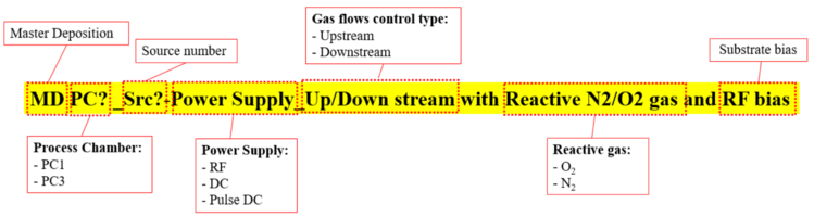
| MD PC1 Src1 RF Upstream | SiO2 | 3 | 140 (RF) | 2.3 | 0.5 | |
| MD PC1 Src2 RF Upstream | SiO2 | 3 | 140 (RF) | 2.6 | 3 | |
| MD PC1 Src3 DC Upstream | Ni | 3 | 500 (DC) | 23.3 | 2.5 | |
| MD PC1 Src4 DC Upstream | Cu | 3 | 500 (DC) | 52.2 | 2.2 | |
| MD PC1 Src5 DC Upstream | Al | 3 | 200 (DC) | 7.9 | 3.2 | |
| MD PC1 Src5 Pulse DC Downstream with reactive O2 |
Al | 3 | 500 (PDC) Frequency: 100Hz Reverse time: 2µs |
1.7 | 3.4 | Ar flow: 50sccm O2 flow: 15 sccm
|
| MD PC1 Src6 Pulse DC Upstream | ITO | 3 | 140 (PDC) Frequency: 100Hz Reverse time: 2µs |
11 | 4.5 | |
| MD PC1 Src6 Pulse DC Downstream with reactive O2 |
ITO | 3 | 140 (PDC) Frequency: 100Hz Reverse time: 2µs |
11.3 | - | Ar flow: 50sccm O2 flow: 2 sccm |
| MD PC1 Src1 RF Upstream | Si | 3 | 120 (RF) | 1.8 | - | |
| MD PC3 Src1 Pulse DC Downstream with reactive N2 |
Al | 3 | 900 (PDC) Frequency: 100Hz Reverse time: 2µs |
29 | 3.2 | Ar flow: 50sccm O2 flow: 15 sccm |
Substrate heating
During the test by KJLC, using a wafer with thermocouples attached to it, the temperature of the wafer and the control thermocouple could be tracked. In general, the sample will be about 50 degrees less than the temperature displayed on the system. There are software interlocks that control/protect the heater as well as a hardware interlock that will prevent the heater from turning on when the chamber is at atmosphere or if there is insufficient water flow on the system.
There are software interlocks that will not allow the transfer port to open while the heater is on. Also, it will not allow the heater to turn on if there are no assigned wafer in the chamber, and also will not allow the chamber vent valve to open if the temperature shows above 80 degrees Celsius.
There is no sensor to detect if a sample is physically present. If a user transfers an empty wafer carrier into a process chamber, the wafer ID will move accordingly and the heater can be turned on.
A sample transferring can be done while the sample is hot but not while the heater is on. The heater thermocouples will cool very rapidly as soon as the heater is turned off so there is no set temperature. A sample transfer unload should be done when the temperature is below 300 degrees Celsius.
Substrate heating procedure:
There are dedicated recipes to turn on a heater:
- If PC1 is used, select “Master Heater PC1 - On”
- If PC3 is used, select “Master Heater PC3 - On”
Substrate cleaning (RF Bias)
The RF cleaning can be used to clean the sample before the deposition. There are depicted recipes for that:
- If PC1 is used, select “Master Bias PC1_Upstream”
- If PC3 is used, select “Master Bias PC3_Upstream”
The user can select rotation speed (10 rpm), process pressure (1-15mTorr) RF power (maximum 100 W) and cleaning time (maximum 1800 s).