LabAdviser/314/Microscopy 314-307/SEM/Nova/Transmission Kikuchi diffraction: Difference between revisions
| Line 31: | Line 31: | ||
= Orientation Imaging Microscopy = | = Orientation Imaging Microscopy = | ||
The necessity to obtain large data sets of crystal orientations and crystallographic | The necessity to obtain large data sets of crystal orientations and crystallographic phases in polycrystalline materials, the development of electron microscopy, together with the perfecting of automated Kikuchi pattern indexing, led in the last 20 years to the development of a powerful new form of microscopy, the so-called Orientation Imaging Microscopy (OIM). OIM generally refers to techniques for the reconstruction of micro- and nanostructures based on the spatially resolved measurement of individual crystal orientations and crystallographic phases. | ||
phases in polycrystalline materials, the development of electron | |||
microscopy, together with the perfecting of automated Kikuchi pattern indexing, | |||
led in the last 20 years to the development of a powerful new form | |||
of microscopy, the so-called Orientation Imaging Microscopy (OIM) | |||
OIM generally refers to techniques for the reconstruction of micro- and | |||
nanostructures based on the spatially resolved measurement of individual | |||
crystal orientations and crystallographic phases | |||
Electron diffraction techniques are particularly suited for such analysis because they allow (i) unambiguous orientation determination, (ii) orientation and phase determination | |||
for all crystal systems, (iii) high spatial resolutions and (iv) high automatization. OIM can be performed using both SEM and TEM instruments; a schematic representation of an OIM system inside a SEM is shown in Fig. 4. | |||
While a pole | In an OIM scan the beam is stepped across the sample surface in a regular grid. The user typically programs an array of positions, specifying the spatial range and step size of sampling points. At each point the Kikuchi pattern is captured and automatically indexed in real time and the orientation and other information recorded. The acquired OIM data are usually plotted in the form of an inverse pole figure (IPF) orientation map, an example of which is shown in Fig. 5. | ||
material within the sample reference system, an inverse pole | |||
<gallery widths="350px" heights="250px" perrow="2" halign="center"> image:Picture10.png|Fig. 3: the base with the micromanipulator mounted on it. | |||
the crystal system, in most cases the inverse pole | image:Picture25.png|Fig. 4: the micromanipulator mounted on the Nova NanoSEM door. </gallery> | ||
example it is a standard triangle in the case of cubic materials. Thus, IPF | |||
coloring of OIM data shows which crystal direction is parallel to the sample | While a pole figure represents a crystal direction or plane normal of a material within the sample reference system, an inverse pole figure displays a specific sample direction within the crystal system. Due to the symmetry of the crystal system, in most cases the inverse pole figure can be reduced, for example it is a standard triangle in the case of cubic materials. Thus, IPF coloring of OIM data shows which crystal direction is parallel to the sample direction to which the IPF is assigned to. Using the common color-code for | ||
direction to which the IPF is assigned to. Using the common color-code for | cubic materials, [100] points parallel to the assigned sample direction are colored red, [110] green and [111] blue, while mixtures of orientations are colored in mixed colors. | ||
cubic materials, [100] points parallel to the assigned sample direction are | |||
colored red, [110] green and [111] blue, while mixtures of orientations are | The first-developed and most popular SEM OIM technique is the electron backscatter diffraction (EBSD). In the TEM the main techniques used are the transmission Kikuchi pattern (TKP) technique, the small-angle convergent beam diffraction (SCBED) and the precession enhanced diffraction (PED) method. | ||
colored in mixed colors. | |||
The | |||
backscatter | |||
techniques used are the transmission Kikuchi pattern (TKP) technique, the | |||
small-angle convergent beam | |||
= On-axis Transmission Kikuchi diffraction = | = On-axis Transmission Kikuchi diffraction = | ||
Revision as of 12:16, 8 August 2018
Kikuchi lines
The formation of Kikuchi patterns can be described as a two-step process, as shown schematically in Fig. 1. The first step consists of an incoherent inelastic, large angle scattering process of the primary beam electrons, producing a point-like electron source inside of the crystal. The second step is the elastic and inelastic coherent scattering of these electrons by the crystal planes of the material: the electrons can be Bragg reflected at lattice planes with reciprocal lattice vector -g if the Bragg angle is ±θB or if the direction of incidence kθ lies on one of the Kossel cones, which have an aperture 90°- θB and the g direction (normal to the lattice planes) as axis. There is a pair of Kossel cones for g, another pair for 2g and so on. The intersection between the Kossel cones and the plane of observation results in the formation of Kikuchi lines. The intersection is an hyperbola, but the lines are approximately straight owing to the low value of θB. The formed Kikuchi lines do not have the same intensity: one line, called the excess line, is brighter than the other, called the defect line. An example of a formed Kikuchi pattern is visible in Fig. 2, showing the excess (bright) and defect (black) Kikuchi lines and a zone axis, indicating an intersection of planes.
-
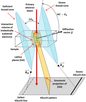 Fig. 1: Schematic representation of Kikuchi lines formation.
 -
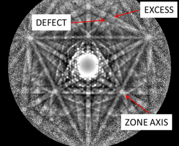 Fig. 2: Image of a Kikuchi pattern from an Au thin-film, recorded on a FEI Nova 600 NanoSEM at 30 kV acceleration voltage.


The simple geometry of Kikuchi diffraction makes indexing and orientation determination from Kikuchi patterns straightforward: the position of the diffracting lattice plane in the crystal can be easily determined from the center line of a pair of Kikuchi lines, together with the lattice plane spacing from the distance between the lines themselves.
Indexing of Kikuchi patterns
The automated determination of the position of Kikuchi lines in a diffraction pattern (and consequently of lattice planes in the crystal) has enabled the practical use of Kikuchi diffraction for the study of micro- and nanomaterials. An algorithm known as the Hough transform was introduced by Krieger Lassen to recognize the edges of the Kikuchi bands [1,2]. The Hough transform is a mathematical tool which can be used to isolate features of a particular shape, such as lines, circles and ellipses, within an image. The main advantage of the Hough transform is that it is relatively unaffected by image noise. The essential idea of the the Hough transform consists of applying to each pixel of the Kikuchi pattern the equation:
ρi = xcosθi + ysinθi (1)
where (x, y) are the coordinates of a pixel in the original image and (ρi, θi) are the parameters of a straight line passing through (x, y). From Eq. 1 it is evident that the set of possible lines passing through the chosen pixel is represented by a sinusoid in the Hough space.
An example is shown in Fig. 3. Consider four pixels along a Kikuchi line. For each pixel in the line, all possible values of ρ are calculated for θ ranging from 0° to 180° using Eq. 1, which produces four sinusoidal curves. These curves intersect at a point with (ρ, θ) coordinates (green rectangle), corresponding to the angle of the line (θ) and its position relative to the origin (ρ). The grey-scale intensity I(xi; yi) of the image pixels is accumulated in each quantized point H(ρ; θ) of the Hough space, so that I(xi; yi) serves as a measure of evidence for a line passing through the pixel (x, y). In this way, a line in the pattern space transforms to a point having a certain intensity in the Hough space, which is easily detected by the indexing software over the at background. For a correct indexing, the crystal system, chemical composition, unit cell dimensions and atomic positions of the material must be supplied to the analysis software.

In a Kikuchi pattern, a set of orientations is obtained from a triplet of bands by measuring the interplanar angles between the bands. These values are compared against theoretical values of all angles formed by various planes for a given crystal system. When the (h, k, l ) values of a pair of lines are identified, they give information about the pair of planes, but that does not permit to distinguish between the two planes. At least three sets of lines are required to completely identify the individual planes and hence to find the orientation of the sample. For a given number of bands, n, used for pattern indexing, the number of band triplets is determined by the following formula:
N.triplets = n!/(n - 3)! * 3! (2)
Typically from 3 to 9 detected bands are used for automatic indexing in commercial softwares.
Orientation Imaging Microscopy
The necessity to obtain large data sets of crystal orientations and crystallographic phases in polycrystalline materials, the development of electron microscopy, together with the perfecting of automated Kikuchi pattern indexing, led in the last 20 years to the development of a powerful new form of microscopy, the so-called Orientation Imaging Microscopy (OIM). OIM generally refers to techniques for the reconstruction of micro- and nanostructures based on the spatially resolved measurement of individual crystal orientations and crystallographic phases.
Electron diffraction techniques are particularly suited for such analysis because they allow (i) unambiguous orientation determination, (ii) orientation and phase determination for all crystal systems, (iii) high spatial resolutions and (iv) high automatization. OIM can be performed using both SEM and TEM instruments; a schematic representation of an OIM system inside a SEM is shown in Fig. 4.
In an OIM scan the beam is stepped across the sample surface in a regular grid. The user typically programs an array of positions, specifying the spatial range and step size of sampling points. At each point the Kikuchi pattern is captured and automatically indexed in real time and the orientation and other information recorded. The acquired OIM data are usually plotted in the form of an inverse pole figure (IPF) orientation map, an example of which is shown in Fig. 5.
-
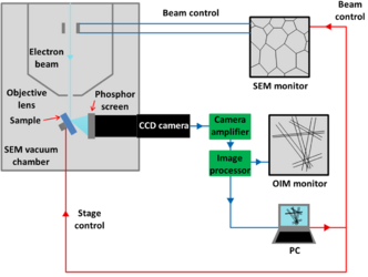 Fig. 3: the base with the micromanipulator mounted on it.
 -
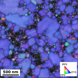 Fig. 4: the micromanipulator mounted on the Nova NanoSEM door.


While a pole figure represents a crystal direction or plane normal of a material within the sample reference system, an inverse pole figure displays a specific sample direction within the crystal system. Due to the symmetry of the crystal system, in most cases the inverse pole figure can be reduced, for example it is a standard triangle in the case of cubic materials. Thus, IPF coloring of OIM data shows which crystal direction is parallel to the sample direction to which the IPF is assigned to. Using the common color-code for cubic materials, [100] points parallel to the assigned sample direction are colored red, [110] green and [111] blue, while mixtures of orientations are colored in mixed colors.
The first-developed and most popular SEM OIM technique is the electron backscatter diffraction (EBSD). In the TEM the main techniques used are the transmission Kikuchi pattern (TKP) technique, the small-angle convergent beam diffraction (SCBED) and the precession enhanced diffraction (PED) method.