LabAdviser/314/Microscopy 314-307/SEM/Nova/Transmission Kikuchi diffraction
Feedback to this page: click here
This work was performed by PhD student Matteo Todeschini during period 2014-2017 (content created by Matteo Todeschini @DTU Nanolab, 2017)
Formation of Kikuchi lines
The formation of Kikuchi patterns can be described as a two-step process, as shown schematically in Fig. 1. The first step consists of an incoherent inelastic, large angle scattering process of the primary beam electrons, producing a point-like electron source inside of the crystal. The second step is the elastic and inelastic coherent scattering of these electrons by the crystal planes of the material: the electrons can be Bragg reflected at lattice planes with reciprocal lattice vector -g if the Bragg angle is ±θB or if the direction of incidence kθ lies on one of the Kossel cones, which have an aperture 90°- θB and the g direction (normal to the lattice planes) as axis. There is a pair of Kossel cones for g, another pair for 2g and so on. The intersection between the Kossel cones and the plane of observation results in the formation of Kikuchi lines. The intersection is an hyperbola, but the lines are approximately straight owing to the low value of θB. The formed Kikuchi lines do not have the same intensity: one line, called the excess line, is brighter than the other, called the defect line. An example of a formed Kikuchi pattern is visible in Fig. 2, showing the excess (bright) and defect (black) Kikuchi lines and a zone axis, indicating an intersection of planes.
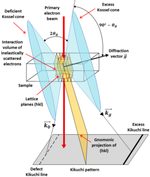
Fig. 1: Schematic representation of Kikuchi lines formation.
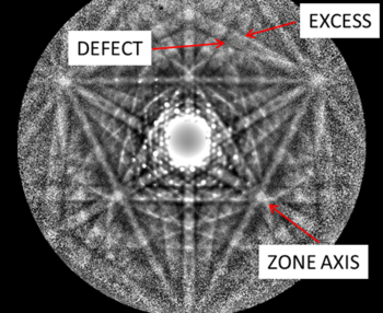
Fig. 2: Image of a Kikuchi pattern from an Au thin-film, recorded on a FEI Nova 600 NanoSEM at 30 kV acceleration voltage.


The simple geometry of Kikuchi diffraction makes indexing and orientation determination from Kikuchi patterns straightforward: the position of the diffracting lattice plane in the crystal can be easily determined from the center line of a pair of Kikuchi lines, together with the lattice plane spacing from the distance between the lines themselves.
Indexing of Kikuchi patterns
The automated determination of the position of Kikuchi lines in a diffraction pattern (and consequently of lattice planes in the crystal) has enabled the practical use of Kikuchi diffraction for the study of micro- and nanomaterials. An algorithm known as the Hough transform was introduced to recognize the edges of the Kikuchi bands. The Hough transform is a mathematical tool which can be used to isolate features of a particular shape, such as lines, circles and ellipses, within an image. The main advantage of the Hough transform is that it is relatively unaffected by image noise. The essential idea of the the Hough transform consists of applying to each pixel of the Kikuchi pattern the equation:
ρi = xcosθi + ysinθi (1)
where (x, y) are the coordinates of a pixel in the original image and (ρi, θi) are the parameters of a straight line passing through (x, y). From Eq. 1 it is evident that the set of possible lines passing through the chosen pixel is represented by a sinusoid in the Hough space.
An example is shown in Fig. 3. Consider four pixels along a Kikuchi line. For each pixel in the line, all possible values of ρ are calculated for θ ranging from 0° to 180° using Eq. 1, which produces four sinusoidal curves. These curves intersect at a point with (ρ, θ) coordinates (green rectangle), corresponding to the angle of the line (θ) and its position relative to the origin (ρ). The grey-scale intensity I(xi; yi) of the image pixels is accumulated in each quantized point H(ρ; θ) of the Hough space, so that I(xi; yi) serves as a measure of evidence for a line passing through the pixel (x, y). In this way, a line in the pattern space transforms to a point having a certain intensity in the Hough space, which is easily detected by the indexing software over the at background. For a correct indexing, the crystal system, chemical composition, unit cell dimensions and atomic positions of the material must be supplied to the analysis software.

In a Kikuchi pattern, a set of orientations is obtained from a triplet of bands by measuring the interplanar angles between the bands. These values are compared against theoretical values of all angles formed by various planes for a given crystal system. When the (h, k, l ) values of a pair of lines are identified, they give information about the pair of planes, but that does not permit to distinguish between the two planes. At least three sets of lines are required to completely identify the individual planes and hence to find the orientation of the sample. For a given number of bands, n, used for pattern indexing, the number of band triplets is determined by the following formula:
N.triplets = n!/(n - 3)! * 3! (2)
Typically from 3 to 9 detected bands are used for automatic indexing in commercial softwares.
Orientation Imaging Microscopy
The necessity to obtain large data sets of crystal orientations and crystallographic phases in polycrystalline materials, the development of electron microscopy, together with the perfecting of automated Kikuchi pattern indexing, led in the last 20 years to the development of a powerful new form of microscopy, the so-called Orientation Imaging Microscopy (OIM). OIM generally refers to techniques for the reconstruction of micro- and nanostructures based on the spatially resolved measurement of individual crystal orientations and crystallographic phases.
Electron diffraction techniques are particularly suited for such analysis because they allow (i) unambiguous orientation determination, (ii) orientation and phase determination for all crystal systems, (iii) high spatial resolutions and (iv) high automatization. OIM can be performed using both SEM and TEM instruments; a schematic representation of an OIM system inside a SEM is shown in Fig. 4.

In an OIM scan the beam is stepped across the sample surface in a regular grid. The user typically programs an array of positions, specifying the spatial range and step size of sampling points. At each point the Kikuchi pattern is captured and automatically indexed in real time and the orientation and other information recorded. The acquired OIM data are usually plotted in the form of an inverse pole figure (IPF) orientation map, an example of which is shown in Fig. 5.

While a pole figure represents a crystal direction or plane normal of a material within the sample reference system, an inverse pole figure displays a specific sample direction within the crystal system. Due to the symmetry of the crystal system, in most cases the inverse pole figure can be reduced, for example it is a standard triangle in the case of cubic materials. Thus, IPF coloring of OIM data shows which crystal direction is parallel to the sample direction to which the IPF is assigned to. Using the common color-code for cubic materials, [100] points parallel to the assigned sample direction are colored red, [110] green and [111] blue, while mixtures of orientations are colored in mixed colors.
On-axis Transmission Kikuchi diffraction
This technique is based on the collection of Kikuchi patterns from electron transparent samples. In 2016 the on-axis TKD configuration was presented. In this system the detector is located perpendicularly beneath the electron transparent sample on the optical axis of the microscope, obtaining an instrument resolution almost the same as that using Kikuchi patterns in TEM. A schematic illustration of the detector is shown in Fig. 6.

Moving the detector to the on-axis position permits to reduce the probe current and size to record a solvable pattern. Kikuchi patterns are more intense at small scattering angles (i.e., near the direction of the optical axis) than at higher angles. Therefore, the intensity of the incident electron beam, and thus the probe size needed to record a solvable pattern is smaller when the detector is moved from a high-angle to the on-axis position. The probe size in combination with the beam broadening affect the total interaction volume, and the width of the interaction volume is directly linked to the lateral resolution. All the experiments and results presented in the next section were obtained using the on-axis detector configuration, which has already become the standard geometry for TKD measurements.
In-situ heating TKD analysis of ultra-thin metal films
Solid-state dewetting
In this section, the in-situ and high temperatures capabilities of TKD for the analysis of metal thin-films are presented. The model example chosen for this analysis is the solid-state dewetting of Au thin-films. Solid-state dewetting is a morphological evolution by which an initially continuous thin film on an inert substrate turns into a discontinuous array of isolated islands, as sketched in Fig. 7.

This happens because thin films are kinetically frozen unstable structures as a consequence of their formation far from equilibrium. Since the driving force for dewetting is the minimization of the total energy of the free surfaces of the film and substrate and of the film-substrate interface, the total free energy associated with the interfaces of a film is reduced if the film agglomerates to form islands. Solid-state dewetting occurs at temperatures well below the melting temperature of the film, so that the material remains in the solid state throughout the process. Since the rate of dewetting is higher in thinner films, the temperature at which dewetting occurs decreases with decreasing film thickness.
Nanostructure evolution during heating
Figures 8 and 9 show the IPFZ maps overlaid with pattern quality for temperatures varying from 20°C to 900°C. A preliminary investigation of the Au film at room temperature revealed a bimodal nanostructure, with the presence of small grains with size in the range of 30 nm and large grains with size in the 150 nm range. The latter ones showed a strong [111] out-of-plane texture. During heating, the [111] grains tended to grow faster than the [110] and [100] ones. It is also possible to observe that grain growth started at a temperature below 150°C, while holes are visible at 170°C (highlighted with a red circle). The holes were formed in the vicinity of non-preferentially oriented (non-PO) [110] and [100] grains, which were also the site where the hole growth was continuing.
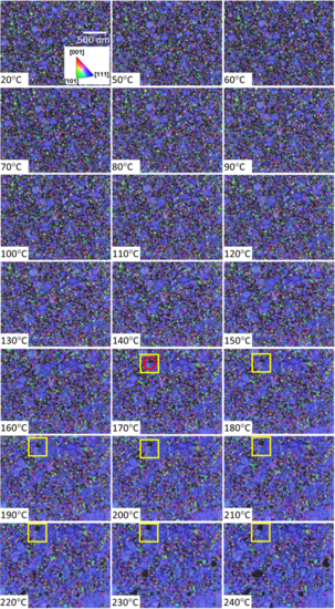
Fig. 8: IPFZ maps of the 15 nm Au film, overlaid with pattern quality map, recorded at temperatures between 20°C and 240°C.
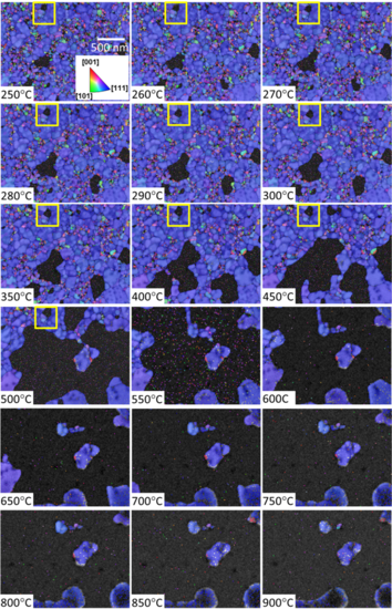
Fig. 9: IPFZ maps of the 15 nm Au film, overlaid with pattern quality map, recorded at temperatures between 250°C and 900°C.


The yellow rectangles follow instead the delayed hole growth due to the presence of preferentially oriented (PO) [111] grains: the hole is visible from 170°C and grows until it is completely surrounded by larger PO grains, subsequently its growth is retarded until 500°C, while other holes continue to grow. When a hole meets a grain having a low interface energy (in this case a [111] grain), edge retraction is inhibited due to the reduced driving force for dewetting, because these grains are energetically very stable. The low-interface energy grains, which inhibited the retraction, continue to grow at the expense of neighboring grains having higher interface energy, resulting in abnormal grain growth, and the hole continues to grow in directions where grains along the hole edge have a higher interface energy with the substrate. This expansion only stops when the hole becomes completely sorrounded by low-interface energy grains, as in the case of Fig. 8 and 9.
Since TKD measurements provided a large amount of data for each scanned point in the map (54000 total acquired points at the step size of 10 nm), statistically significant quantitative data analysis could be performed from this series of measurements. The two classes of grains already observed in Fig. 8 and 9 were analyzed, defined as i) PO-grains with [111]//growth direction (using tolerance angle of 15°) and ii) non-PO grains with other orientations. The average grain size evolution of both classes of grains is shown in Fig. 10a for annealing temperatures up to 600°C.
The graph confirms the trend from the maps shown in Fig. 8, revealing that grain growth started already at 120°C. The PO grains were larger than the non-PO ones already from the starting nanostructure and grew considerably faster: by a temperature of 220°C, PO grains have almost triplicated their average size, while non-PO grains maintained their average size of 33 nm. Furthermore, up to 550°C practically only the PO grains grew. Fig. 10b shows the evolution of the number of indexed points for the two classes of grains, while Fig. 10c shows the number of grains of each class during annealing. The data shows that the fraction of indexed points and the number of non-PO grains started to decrease at the annealing temperature of 150°C. Considering that the holes were formed near non-PO grains as described above, the decrease of non-PO indexed points can be considered as a signal of hole formation in the film, even if holes are not visible in the image at that temperature. For PO grains, the fraction of indexed points kept increasing up to 350°C, while the number of grains already started to decrease at 180°C, indicating that such grains kept growing and coalescing before the dewetting process took place.

Determination of the temperature of formation of the first hole
The holes in the film formed near non-preferentially oriented (non-PO) [110] and [100] grains and it was initially supposed that the decrease of non-PO indexed points from a temperature of 150°C could be considered as a signal of hole formation in the film, even if the holes were not yet visible in the map. However, the indexed point number criterion alone is not enough to evaluate the starting point of the dewetting, because the total number of indexed points is a convolution of i) points that were initially indexed, but became not indexed with temperature due to the dewetting of the material and ii) points that were initially not indexed, due to the relatively large value of step sized used, but which started to get indexed with temperature when the growing grains became bigger than the step size.
Therefore it has been necessary to find another reliable evaluation criterion to confirm the exact starting temperature of formation of the holes in the film. The new criterion used consisted in the evaluation of the quality of the Kikuchi patterns on the non-indexed areas of the map. Fig. 11a shows the IPFZ map acquired at 210°C: in this map there are several non-mapped (and therefore black) areas. Fig. 11b shows the Kikuchi pattern recorded from a dewetted area of the sample, while Fig. 11c shows the pattern from an area with very fine grains (in the range of 10-20 nm). The difference between those two patterns is evident. In c) the Kikuchi pattern is visible, but indexing was difficult due to the chosen step size and to the fact that the grain size was close to the physical resolution of the TKD technique; thus many patterns originated from grain boundaries were difficult to be indexed. In b) no pattern is instead visible, indicating lack of crystalline material, i.e. only the Si3N4 substrate was present at that position.
