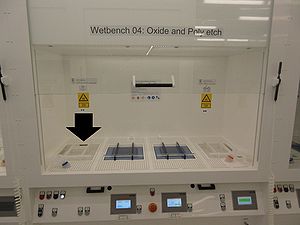
Specific Process Knowledge/Etch/Wet Polysilicon Etch: Difference between revisions
| Line 21: | Line 21: | ||
<!-- remember to remove the type of documents that are not present --> | <!-- remember to remove the type of documents that are not present --> | ||
[http://labmanager.danchip.dtu.dk/function.php?module=Machine&view=view&mach=379 | [http://labmanager.danchip.dtu.dk/function.php?module=Machine&view=view&mach=379 Poly Si Etch info page in LabManager] | ||
===PolySi Etch data=== | ===PolySi Etch data=== | ||
Revision as of 11:04, 3 August 2018
Feedback to this page: click here
Wet PolySi Etch

The wet PolySi Etch is an isotropic silicon etch. This holds for both a poly-silicon thin-film as well as single-crystalline material such as a Si(100) surface. The Poly Si Etch bath is placed inside 'Wet Bench 04: Oxide and Poly etch' cleanroom D-3. For samples that are not allowed in this bath the polysilicon etch solution can also be mixed in a plastic beaker in Fume hood 01 or 02 (Acids/bases).
The PolySi Etch is typically used for opening holes in poly-silicon thin-films, using photoresist as an etch mask or to strip Poly silicon of a wafer. Due to its isotropic nature the under-etching (etch-bias) at least amounts to the thickness of the poly-silicon layer. Another example of usage is etching of "circular-shaped" holes in silicon substrates.
The PolySi Etch is based on the combined oxidation of silicon followed by dissolution of the silicon oxide. The etch solution consists of:
HNO3 : BHF : H2O - (20 : 1 : 20)
NB: The life time of the solution is a few days to one week.
The user manual and contact information can be found in LabManager:
Poly Si Etch info page in LabManager
PolySi Etch data
| PolySi Etch @ room temperature | |
|---|---|
| General description |
Etch of poly-si/Si(100) |
| Chemical solution | HNO3 : BHF : H2O (20 : 1 : 20) |
| Process temperature | Room temperature |
| Possible masking materials |
|
| Etch rate |
|
| Batch size |
1-25 wafers at a time |
| Size of substrate |
4-6" wafers |
