LabAdviser/Technology Research/Fabrication of Hyperbolic Metamaterials using Atomic Layer Deposition/AZO pillars: Difference between revisions
| Line 4: | Line 4: | ||
Tempress) based on SiH<sub>4</sub> at 560 °C. This procedure enables the preparation of home-made silicon-on-insulator (SOI) substrates. | Tempress) based on SiH<sub>4</sub> at 560 °C. This procedure enables the preparation of home-made silicon-on-insulator (SOI) substrates. | ||
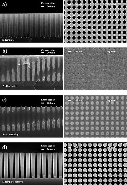
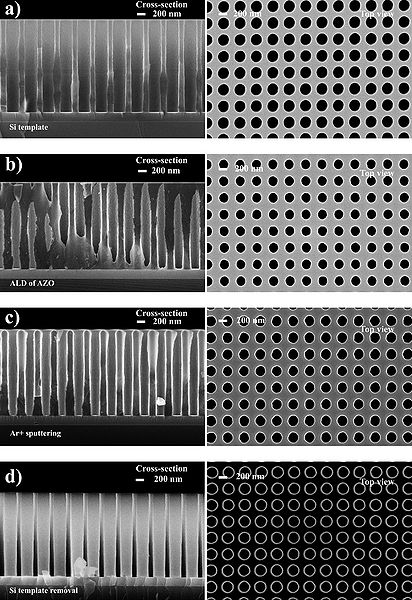
The main steps in the fabrication of pillars and tubes are shown in Fig 1. Initially, silicon holes were etched in SOI wafers by deep-UV lithography and DRIE (Fig. 1(a)-1(c)). The holes were arranged in a square lattice with the pitch of 400 nm. The template was then filled with an ALD D25 AZO coating (Fig. 1(d)) at 250 °C. The thickness of the deposited AZO depends on the desired output. An entire filling would result in the formation of pillars, while partial deposition leads to fabrication of hollow tubes. After removal of the top parts by Ar+ ion sputtering (Fig. 1(e)), the silicon core between the ALD coated holes was etched away during the last step. Figure 1(f) represents the final structures. Fabrication output is shown in Fig. 2. Each process step was carefully analyzed using cross-sectional SEM imaging (see Figs. 3 and 4 for tubes | The main steps in the fabrication of pillars and tubes are shown in Fig 1. Initially, silicon holes were etched in SOI wafers by deep-UV lithography and DRIE (Fig. 1(a)-1(c)). The holes were arranged in a square lattice with the pitch of 400 nm. The template was then filled with an ALD D25 AZO coating (Fig. 1(d)) at 250 °C. The thickness of the deposited AZO depends on the desired output. An entire filling would result in the formation of pillars, while partial deposition leads to fabrication of hollow tubes. After removal of the top parts by Ar+ ion sputtering (Fig. 1(e)), the silicon core between the ALD coated holes was etched away during the last step. Figure 1(f) represents the final structures. Fabrication output is shown in Fig. 2. Each process step was carefully analyzed using cross-sectional SEM imaging (see Figs. 3 and 4 for pillars and tubes fabrication, respectively). | ||
<br clear="all" /> | <br clear="all" /> | ||
| Line 14: | Line 14: | ||
<gallery caption="" widths="500px" heights="600px" perrow="2"> | <gallery caption="" widths="500px" heights="600px" perrow="2"> | ||
image: | image:AZO_pillars_fab_supplementary_eves.jpg| Figure 3. SEM verification for each fabrication step of pillars production. Left side shows cross-sectional images and right side of the Figure shows the top view of the structures. | ||
image: | image:AZO_tubes_fab_supplementary_eves.jpg| Figure 4. SEM verfication for each fabrication step of tube production. Left side shows cross-sectional images and right side of the Figure shows the top view of the structures. | ||
</gallery> | </gallery> | ||
Revision as of 19:30, 15 March 2017
Procces flow description
Double side polished (DSP), 150 mm (100) Si wafers were selected for device fabrication. They were RCA cleaned and later oxidized in a conventional quartz tube (furnace from Tempress) using a dry oxidation process based on O2 at 1100 °C, resulting in a 200 nm SiO2 layer on Si. Next, a 2 μm amorphous Si layer was deposited on the SiO2 surface using a conventional low-pressure chemical vapor deposition (LPCVD) process (furnace from Tempress) based on SiH4 at 560 °C. This procedure enables the preparation of home-made silicon-on-insulator (SOI) substrates.
The main steps in the fabrication of pillars and tubes are shown in Fig 1. Initially, silicon holes were etched in SOI wafers by deep-UV lithography and DRIE (Fig. 1(a)-1(c)). The holes were arranged in a square lattice with the pitch of 400 nm. The template was then filled with an ALD D25 AZO coating (Fig. 1(d)) at 250 °C. The thickness of the deposited AZO depends on the desired output. An entire filling would result in the formation of pillars, while partial deposition leads to fabrication of hollow tubes. After removal of the top parts by Ar+ ion sputtering (Fig. 1(e)), the silicon core between the ALD coated holes was etched away during the last step. Figure 1(f) represents the final structures. Fabrication output is shown in Fig. 2. Each process step was carefully analyzed using cross-sectional SEM imaging (see Figs. 3 and 4 for pillars and tubes fabrication, respectively).
-
Figure 1. Schematics of the fabrication flow. a) Home-made SOI substrates. b) Deep-UV lithography. Resist spin coating, baking, exposure and developing. c) DRIE etching, fabrication of initial Si template. d) ALD deposition of D25 AZO at 250 °C. Partial deposition will lead to fabrication of tubes, while complete filling will create full pillars. e) Removal of the top AZO layer by Ar+ sputtering. f) Silicon host removal using conventional RIE process.
-
Figure 2. SEM images, bird-eye-view. a) AZO pillars and b) AZO tubes.
-
Figure 3. SEM verification for each fabrication step of pillars production. Left side shows cross-sectional images and right side of the Figure shows the top view of the structures.
-
Figure 4. SEM verfication for each fabrication step of tube production. Left side shows cross-sectional images and right side of the Figure shows the top view of the structures.


